Robust Contact Monitor Simplif


Abstract: This application note demonstrates how the MAX13362 automotive switch monitor performs during ECU-level testing. The article describes the tests performed and the results obtained.
This article documents how the MAX13362 reacts in many circumstances encountered during automotive ECU-level testing. The situations described here are presented in the following sections:
During testing special attention was paid t 1) possible undesired leakage currents due to voltage differences; 2) whether SPI communication was possible; and 3) whether switch status was reported correctly or incorrectly. All tests were conducted with a battery voltage of 14V.
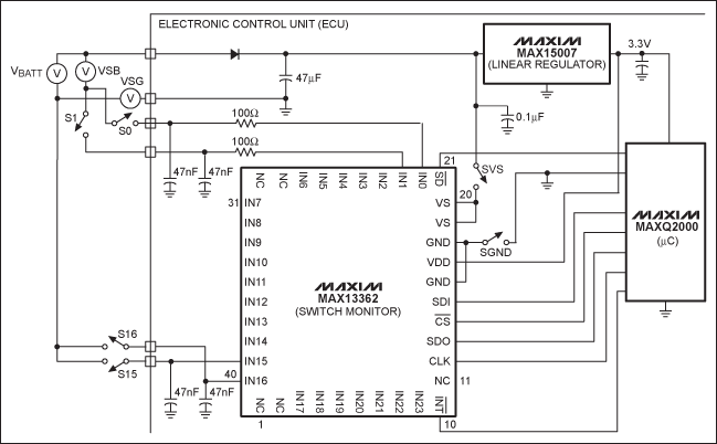
Figure 1. The MAX13362 test circuit.
1.1. Loss of Ground
When loss of ground occurs (for example, due to a bad solder joint), it can happen with one or more of the external switches open or shorted to either battery or chassis ground. Thus a number of different loss-of-ground situations need to be considered:
1.1.1. With All Switches Open
After powering-up in the normal way, the IC ground pin was disconnected and the GND pin was observed to float upwards to approximately 0.5V. This allowed the SPI interface to appear to function properly, although with the logic-low level at 0.5V. Depending on the logic levels expected by the processor, this situation could lead to false reads, i.e., where the processor interprets 0.5V as a logic high. This error can happen even though the SPI interface reports the correct output word (0xC0000000), thus indicating that all switches are indeed open (Figure 2). No increase in power-supply current was observed during this test. When the ground connection was restored, the MAX13362 functioned normally.
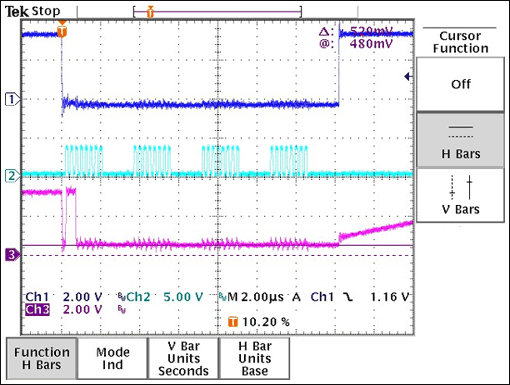
Figure 2. SPI readback shows ground shift. Ch1 = CS; Ch2 = CLK; Ch3 = SDO (data).
1.1.2. With at Least One Input Connected to Chassis Ground
This test was also performed by disconnecting ground after the MAX13362 had been powered up and configured normally. An SPI read reported all switches open. The ground level on the logic interface was shifted upwards by around 600mV, as seen in the previous test. When the ground connection was restored, the MAX13362 functioned normally.
1.2. Loss of Power with an Input Connected to Battery Voltage
To perform this test the VS pin was disconnected from the supply and IN1 was shorted to the battery voltage. The current into the IN1 pin remained at the leakage current level, thus indicating that the VS node was not being pulled up. This configuration avoided the problem of powering up the MAX13362, or any attached circuitry, in an unknown and unpredictable state. The current into the VDD pin was also observed to be unchanged. Reading from the SPI interface in this mode yielded 0x00000000, as the high-voltage section of the MAX13362 was powered down. These results show that if the microcontroller reads from the MAX13362 when it is in this state, then the microcontroller could easily establish that there is a fault.
1.3. Loss of Ground and Power with One Input Grounded
In this test both the VS and the GND pins of the MAX13362 were disconnected and one of the inputs was connected to ground with a switch. Clearly the MAX13362 does not normally operate in this situation, but there was no increase in input current beyond leakage. A read from the SPI interface again yielded 0x00000000, which signaled a fault to the microcontroller.
1.4. Loss of Ground and Power with One Input Connected to Battery Voltage
With the ground and VS pins of the MAX13362 still disconnected, one of the inputs was connected to the battery voltage. Similarly to test 1.2 above, there was no noticeable increase in input current. The VS pin remained at 0V. As expected, a read from the SPI interface resulted in 0x00000000.
1.5. Loss of Ground and Power with One Input Connected to Battery and One Input Grounded
This test was performed to ensure that the MAX13362 would not power up with an input connected to battery and another connected to ground. The desired outcome was confirmed: VS remained at 0V and when the MAX13362 was read, it reported 0x00000000.
2.1. Reverse Battery with All Switches Open
This is the least dangerous condition. The MAX13362 survived it easily, as no abnormal voltages were applied to it.
2.2. Reverse Battery with One Input Grounded
This test is again comparatively benign as no unexpected voltages were applied to the pins of the MAX13362. While the MAX13362 did not, really cannot function, it was not damaged.
2.3. Reverse Battery with One Input Connected to Battery
This is potentially a hazardous situation for the MAX13362 because a negative voltage is applied to one of its inputs while it is not powered. A typical IC with an absolute maximum rating of -0.3V on its inputs would not survive this condition. The MAX13362, however, utilizes special input structures without the usual diodes to ground. This design allows it to survive this condition unscathed. Although the input current on the reversed input remained "leakage-like," the MAX13362 survived this condition for an extended period. An SPI read in this test resulted in 0x00000000.
2.4. Reverse Battery with One Input Connected to Ground and One to Battery
This test was performed and results similar to the previous test (section 2.3) were expected. Indeed, that was the case. No increased input currents were measured and an SPI read yielded 0x00000000.
3.1. Negative Ground Shift
During this test the ground of the MAX13362 and the local microprocessor was shifted negatively with respect to the switch ground in steps of 500mV to observe possible erroneous switch-state changes. Testing was performed with one ground-connected switch and one battery-connected switch closed. No incorrect switch states were reported even with a ground shift as high as -5V. All SPI operations worked flawlessly throughout this test.
3.2. Positive Ground Shift
This test was performed with one closed ground-connected switch and one closed battery-connected switch. With a ground shift of 3.2V the ground-connected switch was reported incorrectly as "open." This error occurred because the input threshold of the MAX13362 used in this test was close to 3.2V. The state of the battery-connected switch was reported correctly up to a ground offset of 5V. All SPI operations worked normally during this test.
3.3. Positive Battery Voltage Shift on Battery-Connected Switch
In this test the voltage supplied to an external (closed) battery-connected switch was increased with respect to the battery voltage supplied to the MAX13362 through the reverse-battery-protection diode. The intention was to ensure that no abnormal current flowed into the affected input and that the switch state was correctly determined by the MAX13362. The voltage shift was increased in steps of 500mV up to a maximum of 5V. No malfunction was observed. The switch state read by SPI was consistently correct. In addition, no increase in input current could be measured.
Table 1. Summary of MAX13362 Robustness Test Results
Additional ECU tests were performed and the MAX13362 functioned as expected. It consistently provided a robust automotive switch interface.
Introduction
The MAX13362 is a 24-channel automotive switch monitor. To avoid the necessity of adding numerous external components, which would increase the application cost and possibly make reliable contact-resistance measurement more difficult, the MAX13362 was carefully designed to be robust. The device monitors the status of 24 remote switches in an automobile while withstanding automotive transients and performing well during the many anomalous automotive test conditions. Since the device interfaces to remote switches in the vehicle, it is directly subjected to all the transients observed in the wiring harness of an automobile.This article documents how the MAX13362 reacts in many circumstances encountered during automotive ECU-level testing. The situations described here are presented in the following sections:
- Lost Ground/Power Connections
- Reverse-Battery Condition
- Ground and Power-Supply Shifts
Test Design Setup
The following test data were generated with the simplified application circuit of Figure 1. The MAX13362 was connected to two external battery-connected switches and two external ground-connected switches. The MAX15007 linear regulator provided a regulated voltage for the digital portion of the IC and for the local microcontroller. The pins connected to ground-connected switches were bypassed with 47nF capacitors to ground. Inputs connected to battery-connected switches had an additional series resistance of 100Ω, necessary to limit input current during the harsher transients on the battery line. The microcontroller used to read and write SPI information was a MAXQ2000 running on a 3.3V supply. The switches SGND and SVS served to disconnect the corresponding MAX13362 pins during testing. The voltage sources VSB and VSG allowed the shifting of the battery voltage and ground, respectively.During testing special attention was paid t 1) possible undesired leakage currents due to voltage differences; 2) whether SPI communication was possible; and 3) whether switch status was reported correctly or incorrectly. All tests were conducted with a battery voltage of 14V.
Figure 1. The MAX13362 test circuit.
1. Lost Ground/Power Connections
Depending on whether the external switches are open or closed (and thus connecting the IC input pins to battery or ground), loss of the ground and/or power connection can lead to a number of different scenarios.1.1. Loss of Ground
When loss of ground occurs (for example, due to a bad solder joint), it can happen with one or more of the external switches open or shorted to either battery or chassis ground. Thus a number of different loss-of-ground situations need to be considered:
1.1.1. With All Switches Open
After powering-up in the normal way, the IC ground pin was disconnected and the GND pin was observed to float upwards to approximately 0.5V. This allowed the SPI interface to appear to function properly, although with the logic-low level at 0.5V. Depending on the logic levels expected by the processor, this situation could lead to false reads, i.e., where the processor interprets 0.5V as a logic high. This error can happen even though the SPI interface reports the correct output word (0xC0000000), thus indicating that all switches are indeed open (Figure 2). No increase in power-supply current was observed during this test. When the ground connection was restored, the MAX13362 functioned normally.
Figure 2. SPI readback shows ground shift. Ch1 = CS; Ch2 = CLK; Ch3 = SDO (data).
1.1.2. With at Least One Input Connected to Chassis Ground
This test was also performed by disconnecting ground after the MAX13362 had been powered up and configured normally. An SPI read reported all switches open. The ground level on the logic interface was shifted upwards by around 600mV, as seen in the previous test. When the ground connection was restored, the MAX13362 functioned normally.
1.2. Loss of Power with an Input Connected to Battery Voltage
To perform this test the VS pin was disconnected from the supply and IN1 was shorted to the battery voltage. The current into the IN1 pin remained at the leakage current level, thus indicating that the VS node was not being pulled up. This configuration avoided the problem of powering up the MAX13362, or any attached circuitry, in an unknown and unpredictable state. The current into the VDD pin was also observed to be unchanged. Reading from the SPI interface in this mode yielded 0x00000000, as the high-voltage section of the MAX13362 was powered down. These results show that if the microcontroller reads from the MAX13362 when it is in this state, then the microcontroller could easily establish that there is a fault.
1.3. Loss of Ground and Power with One Input Grounded
In this test both the VS and the GND pins of the MAX13362 were disconnected and one of the inputs was connected to ground with a switch. Clearly the MAX13362 does not normally operate in this situation, but there was no increase in input current beyond leakage. A read from the SPI interface again yielded 0x00000000, which signaled a fault to the microcontroller.
1.4. Loss of Ground and Power with One Input Connected to Battery Voltage
With the ground and VS pins of the MAX13362 still disconnected, one of the inputs was connected to the battery voltage. Similarly to test 1.2 above, there was no noticeable increase in input current. The VS pin remained at 0V. As expected, a read from the SPI interface resulted in 0x00000000.
1.5. Loss of Ground and Power with One Input Connected to Battery and One Input Grounded
This test was performed to ensure that the MAX13362 would not power up with an input connected to battery and another connected to ground. The desired outcome was confirmed: VS remained at 0V and when the MAX13362 was read, it reported 0x00000000.
2. Reverse-Battery Condition
Automotive systems are exposed to a reverse-battery condition when the car battery is connected incorrectly. The electronics in the car need to endure this condition for an extended period until the hapless car owner (or mechanic) realizes that something is not right. The standard way to protect the automobile's electronics is with a reverse-battery diode, which simply blocks the flow of current in a reverse-battery situation. Using the MAX13362, the VS pin is indeed protected in this way. However, depending on the state of the external switches, the MAX13362 can be exposed to the negative voltage. To find any weak points in the MAX13362, a number of tests were performed with a reverse-battery condition in effect.2.1. Reverse Battery with All Switches Open
This is the least dangerous condition. The MAX13362 survived it easily, as no abnormal voltages were applied to it.
2.2. Reverse Battery with One Input Grounded
This test is again comparatively benign as no unexpected voltages were applied to the pins of the MAX13362. While the MAX13362 did not, really cannot function, it was not damaged.
2.3. Reverse Battery with One Input Connected to Battery
This is potentially a hazardous situation for the MAX13362 because a negative voltage is applied to one of its inputs while it is not powered. A typical IC with an absolute maximum rating of -0.3V on its inputs would not survive this condition. The MAX13362, however, utilizes special input structures without the usual diodes to ground. This design allows it to survive this condition unscathed. Although the input current on the reversed input remained "leakage-like," the MAX13362 survived this condition for an extended period. An SPI read in this test resulted in 0x00000000.
2.4. Reverse Battery with One Input Connected to Ground and One to Battery
This test was performed and results similar to the previous test (section 2.3) were expected. Indeed, that was the case. No increased input currents were measured and an SPI read yielded 0x00000000.
3. Ground and Power-Supply Shifts
The switches connected to the MAX13362 are often remote. It is, therefore, important that the IC continues to function properly when there are differences between the local and remote ground (at the switch) or between the local and remote supply voltage. These differences occur due to high currents flowing through the finite resistance (and inductance) of the vehicle ground and the supply wiring. Many automobile manufacturers specify that normal operation be maintained with ground and power supply shifts of 1V or more. The following tests were performed to determine the sensitivity of the MAX13362 to ground and supply shifts. The tests also sought to determine at what level a ground or supply shift became a problem, i.e., gave an incorrect switch-state reading.3.1. Negative Ground Shift
During this test the ground of the MAX13362 and the local microprocessor was shifted negatively with respect to the switch ground in steps of 500mV to observe possible erroneous switch-state changes. Testing was performed with one ground-connected switch and one battery-connected switch closed. No incorrect switch states were reported even with a ground shift as high as -5V. All SPI operations worked flawlessly throughout this test.
3.2. Positive Ground Shift
This test was performed with one closed ground-connected switch and one closed battery-connected switch. With a ground shift of 3.2V the ground-connected switch was reported incorrectly as "open." This error occurred because the input threshold of the MAX13362 used in this test was close to 3.2V. The state of the battery-connected switch was reported correctly up to a ground offset of 5V. All SPI operations worked normally during this test.
3.3. Positive Battery Voltage Shift on Battery-Connected Switch
In this test the voltage supplied to an external (closed) battery-connected switch was increased with respect to the battery voltage supplied to the MAX13362 through the reverse-battery-protection diode. The intention was to ensure that no abnormal current flowed into the affected input and that the switch state was correctly determined by the MAX13362. The voltage shift was increased in steps of 500mV up to a maximum of 5V. No malfunction was observed. The switch state read by SPI was consistently correct. In addition, no increase in input current could be measured.
Conclusion
None of the tests performed here damaged the MAX13362. The data confirm that the MAX13362 IC is very robust, as its design intended. Table 1 summarizes the conclusions from the testing described in this article.Table 1. Summary of MAX13362 Robustness Test Results
| Test | VS/Input Current | MAX13362 State | SPI Read | SPI Write | Comment | |
| 1.1.1 | Loss of ground with all switches open | Current does not change | Appears to operate | C0 00 00 00 | Succeeds | SDO "low" output voltage is raised to 0.5V. |
| 1.1.2 | Loss of ground with at least one input connected to chassis ground | Current does not change | - | C0 00 00 00 | Succeeds | Switch not reported closed. All output bits 0, apart from DT and Rst. |
| 1.2 | Loss of power with an input connected to battery voltage | Current goes to 0 | - | 00 00 00 00 | Fails | |
| 1.3 | Loss of ground and power with one input grounded | Current goes to 0 | - | 00 00 00 00 | Fails | |
| 1.4 | Loss of ground and power with one input connected to battery voltage | Current goes to 0 | - | 00 00 00 00 | Fails | |
| 1.5 | Loss of ground and power with one input connected to battery and one input grounded | Current goes to 0 | - | 00 00 00 00 | Fails | |
| 2.1 | Reverse-battery with all switches open | Current goes to 0 | Inert | - | - | |
| 2.2 | Reverse-battery with one input grounded | Current goes to 0 | Inert | - | - | |
| 2.3 | Reverse-battery with one input connected to battery | None | Inert | - | - | |
| 2.4 | Reverse-battery with one input connected to ground and one to battery | Current goes to 0 | Inert | 00 00 00 00 | Fails | Set up with two power supplies so that SPI read was possible. |
| 3.1 | Negative GND shift at pin 18 | Current does not change | Normal operation | Succeeds | Succeeds with 5V offset | Tested with up to 5V offset and with no malfunction. |
| 3.2 | Positive GND shift at pin 18 | Current does not change | Normal operation | Succeeds | Succeeds with 5V offset | At 3.2V did not detect a closed ground-connected switch; it still worked at 3.1V. High-side switch detection still worked with 5V offset. |
| 3.3 | Positive battery voltage shift on battery-connected switch | Current does not change | Normal operation | Succeeds | Succeeds with 5V offset | No malfunction at up to 5V offset. |
Additional ECU tests were performed and the MAX13362 functioned as expected. It consistently provided a robust automotive switch interface.
SPI is a trademark of Motorola, Inc.
评论