AnalogICsforLowVoltageSystems
Abstract: This article about low-voltage ICs discusses many types of low-voltage ICs, including voltage regulators, data converters, op amps and current monitors, comparators, microprocessor supervisors, voltage references, analog switches, and interface transceivers. It also present information src="/data/attachment/portal/201007/ET32232201007222232091.gif">
Figure 1. The MAX1589 500mA LDO has preset outputs of 0.75V, 1.0V, 1.3V, 1.5V, 2.5V, and 3.0V. The MAX1818 500mA LDO has preset outputs of 1.5V, 1.8V, 2.0V, 2.5V, 3.0V, and 5.0V or an adjustable output from 1.25V to 5V.
The MAX8510 LDO series incorporates several features important in the design of portable equipment: small size (SC70), low dropout voltage (120mV at 120mA), and low supply current (90µA max.). The MAX8510/MAX8511 are preset to a variety of output voltages between 1.5V and 4.5V, while the MAX8512's output voltage can be adjusted with an external divider.
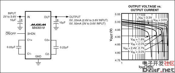
Charge-Pump Voltage ConvertersFor low-current applications, the simplest solution for boosting 3V to 5V is a capacitor-based regulating charge pump (Figure 2). The industry-standard 7660 and most other charge pumps don't regulate VOUT, but the MAX619 includes an analog reference and error amplifier whose output controls a set of internal switches connected to external capacitors. The switch-capacitor network can double or triple VIN, and the MAX619 regulates by switching between these modes of operation. As indicated, this circuit produces 20mA at 5V ±4% for inputs that range between 2V and 3.6V. For inputs between 3.0V and 3.6V, the output-current capability is 50mA.
Figure 2. Occupying less than 0.1in² of board space, the MAX619 regulated charge-pump converter generates 20mA at 5V ±4% for inputs of 2V to 3.6V and 50mA from 3V to 3.6V.
The MAX5008 regulated 5V USB charge pump provides an output current of up to 125mA with supply voltages down to 2.9V, and is suitable for USB host devices with 3.0V or 3.3V supplies.
Systems that handle bipolar signals usually require a negative supply, which can be generated locally if necessary. A simple solution is to use a charge-pump inverter such as the MAX889.
Inductor-Based, Switch-Mode RegulatorsSwitching regulators provide single or multiple outputs. Depending src="/data/attachment/portal/201007/ET32232201007222232093.gif">
Figure 3. The MAX1830 switching regulator converts 3.3V to 1.8V with efficiency greater than 90% from 20mA to 2A, and requires no external MOSFETs.
The MAX1830 comes in a very small, 16-pin QSOP package and has an input range of 3V to 5.5V. Its quiescent operating current drops from 325µA to height=241 alt="Figure 4. The MAX1999 switching regulator generates four output voltages and has two high-efficiency, high-power switch-mode regulators and two low-power linear regulators. It also includes a power-good output, shutdown control, current limiting, and pin-programmable power-up sequencing." src="/data/attachment/portal/201007/ET32232201007222232094.gif" width=590>
Figure 4. The MAX1999 switching regulator generates four output voltages and has two high-efficiency, high-power switch-mode regulators and two low-power linear regulators. It also includes a power-good output, shutdown control, current limiting, and pin-programmable power-up sequencing.
Data ConvertersA/D ConvertersLow power consumption is critical for A/D converters (ADCs) operating in portable equipment. These applications often require high speed, but high speed and low power tend to be mutually exclusive. Accordingly, Maxim produces ADCs that draw moderate supply currents while acquiring data, but very low currents while in shutdown. The result is a power savings for converters that need not operate continuously.
The MAX1115, for example, converts 100k samples per second. It operates from a +3V supply using src="/data/attachment/portal/201007/ET32232201007222232095.gif">
Figure 5. By entering a 1µA power-down mode between conversions, the MAX1115 8-bit ADC offers a dramatic reduction in supply current.
One such application is the measurement of received signal strength in cellular telephones (RSSI: received signal-strength indicator). The MAX1115 digitizes the signal at 2ksps, while drawing a mere 2µA from the 3V supply. Total unadjusted error (the sum of offset, integral nonlinearity, and gain errors) less than 1 LSB and SINAD (signal-to-noise and distortion) less than 48dB are guaranteed.
D/A ConvertersModern D/A converters (DACs) allow low-voltage digital systems to generate analog outputs. Intended for portable applications, these ICs require very little power and board area. The low-cost MAX5811, for instance, is a 10-bit, voltage-output DAC with low 170µA operating current and just 1µA shutdown current, which is ideal for portable applications. Its serial-data control allows it to fit into a SOT23 package.
The MAX5811 operates from single 2.7V supply, and its output swings rail-to-rail. It is ideal for low-cost applications such as trimming offset voltages, setting the bias point for adjustable current (or voltage) sources, and setting the regulation point in other circuits.
Op Amps and Current MonitorsIn op amps, reduced-supply operation reduces the signal-to-noise ratio (SNR) by curtailing the output-voltage swing. Many low-voltage op amps, therefore, offer rail-to-rail output swings as a means of preserving the SNR. For the same reason, many feature an input-voltage range that includes height=280 alt="Figure 6. The MAX4070 bidirectional current-sense amplifier forms a complete current-to-voltage converter." src="/data/attachment/portal/201007/ET32232201007222232096.gif" width=539>
Figure 6. The MAX4070 bidirectional current-sense amplifier forms a complete current-to-voltage converter.
For portable applications that must conserve every microamp, some low-voltage, micropower op amps offer remarkably low supply currents. The +1.4V MAX4036/MAX4038 and +1.8V MAX4474 op amps offer extremely low power consumption at 1.2µA (max). Outputs are rail-to-rail, and input ranges include the negative rail.
Input common-mode voltage range and output voltage swing typically become squeezed when powering op amps from low-voltage supplies. Care must be taken to observe these input and output limits when designing low-voltage circuits. Table 3 presents a cross section of data for the op amps discussed above.
Table 3. A Selection of Specifications for Some of Maxim's Low-Voltage Op Amps PartSupply Voltage
Range (V)Supply Current
(µA, typ/max)Input Common-Mode
Voltage Range (V)Output-Voltage
Swing (V, typ)MAX4036/MAX40381.4 to 3.60.8/1.2VSS to (VDD - 0.4)(VSS + 0.002)
to (VDD - 0.002)MAX40692.7 to 24100/2501.35 to 24(VSS + 0.1)
to (VDD - 0.09)MAX40703.6 to 24100/2501.35 to 24(VSS + 0.1)
to (VDD - 0.09)MAX4236A2.4 to 5.5350/440-0.15 to (VCC - 1.2)(VEE + 0.05)
to (VCC - 0.15)MAX44741.8 to 5.50.75/1.2VSS to (VDD - 1.1)(VSS + 0.001)
to (VDD - 0.004)
ComparatorsLike low-voltage op amps, low-voltage comparators include products separately optimized for high speed, low supply current, and low offset voltage. The MAX9100, for example, is a micropower comparator that operates from a single 1V to 5.5V supply and draws src="/data/attachment/portal/201007/ET32232201007222232097.gif">
Figure 7. The MAX823 offers a supply voltage monitor, a watchdog, and a manual reset all in a single 5-pin SC70/SOT23 package.
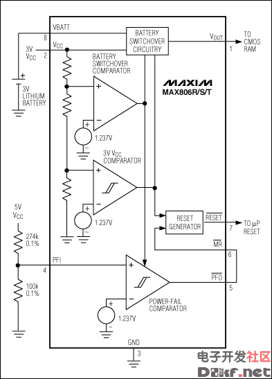
The MAX806R/S/T include battery switchover circuitry and monitor both the 3V and 5V VCC voltages in a dual-voltage system (Figure 8). In this circuit, the main VCC comparator monitors the 3V supply, and the power-fail (PFI) comparator monitors the 5V supply.
Figure 8. Configured as shown, this µP supervisor monitors 5V and 3V VCC in a dual-voltage system.
Internal circuitry issues a reset when the 3V VCC goes out of tolerance. The 5V VCC's trip threshold (4.527V to 4.726V) is set by 0.1% resistors; when 5V falls out of tolerance, the power-fail comparator output (PFO) pulls down the manual-reset input (MR). Thus, an out-of-tolerance condition for either VCC causes the chip to issue a reset.
Some of Maxim's low-voltage supervisors protect the memory ICs with chip-enable (CE) gating. CE gating enables the supervisor to protect the memory by blocking read and write operations during power faults. The MAX792 and MAX820, for example, feature CE gating with a propagation delay through the supervisor of src="/data/attachment/portal/201007/ET32232201007222232099.gif">
Figure 9. The MAX6741 monitors two voltages and generates a reset signal if either drop out of tolerance.
Voltage ReferencesA three-terminal bandgap reference is the best choice when a precision, low-voltage reference with minimal supply current is specified. Three-terminal references generally offer lower operating currents than do the two-terminal zener diodes types (Figure 10).
Figure 10. A three-terminal voltage reference, unlike a two-terminal type, draws constant supply current as the input voltage varies.
Output voltage should be as high as possible for maximum SNR, and the input-to-output voltage difference should be low. A 2.5V reference powered from 3V ±10%, for example, must operate with headroom as low as 200mV. The MAX6029 precision 2.5V reference meets this stringent requirement. It accepts inputs as high as 12V, and draws src="/data/attachment/portal/201007/ET322322010072222320910.gif">
Figure 11. src="/data/attachment/portal/201007/ET322322010072222320911.gif">
Figure 12. The MAX3453 USB transceiver connects low-voltage logic with the 5V USB bus, and is fully USB 1.1/2.0 compliant at 12Mbps and 1.5Mbps.
RS-232 and RS-485RS-232, also known as 232E (officially EIA/TIA-232-E), appeared in the days of mainframe and mini computers, at a time when ±12V power supplies were common, and the original RS-232 transceivers required ±12V for operation. Voltage drops reduced the output swing to about ±9V, so the required minimum was set still lower, at ±5V.
The advent of portable and low-voltage equipment has spawned a new serial-interface specification to replace the old 232E standard, EIA/TIA-562 (562 for brevity). This new standard became effective in 1991. The 562 and 232E standards are electrically compatible, so the new 562 designs will mate with existing 232E equipment and vice versa. Despite the new standard, the term RS-232 lingers, and has come to mean both or either standard in loose parlance.
A comparison of certain 232E and 562 specifications is presented in Table 4. Note that the driver output swings differ (±5V vs. ±3.7V), but the receiver input thresholds are the same (±3V). The 562 devices' ±3.7V minimum output swings allow them to communicate with 232 receivers, which have input thresholds of ±3V. The noise margin, however, is src="/data/attachment/portal/201007/ET322322010072222320912.gif">
Figure 13. This low-voltage interface IC includes a charge pump converter that generates the voltages required for RS-232 communications.


评论