Abstract: This article about low-voltage ICs discusses many types of low-voltage ICs, including voltage regulators, data converters, op amps and current monitors, comparators, microprocessor supervisors, voltage references, analog switches, and interface transceivers. It also present information on power savings and how to manage issues related to low-voltage operation.
Introduction
Low voltages are most appropriate for use in systems where size, weight, and power consumption are especially critical such as PDAs, cell phones, and other battery-operated portable equipment. Low voltages also benefit line-powered systems because the lower power dissipation associated with lower voltage operation allows the use of smaller power supplies, heat-sinks, and fans.Low-voltage ICs are available in many of Maxim's product families including op amps, comparators, microprocessor supervisors, interface, data converters, analog switches and multiplexers, voltage references, DC-DC converters, digital potentiometers, and timing components such as real-time clocks.This discussion covers many of the analog IC families mentioned above, the power savings inherent in their operation, and how to handle some of the issues associated with low-voltage operation. It also presents methods for generating the lower voltages from a 5V supply. Table 1 presents a selection of Maxim's 1.8V, 2.5V, 3.0V, and 3.3V integrated circuits.Table 1. A Selection of Maxim's Low-Voltage Parts
Category
1.8V
2.5V
3V
3.3V
µP Supervisors
MAX6326
MAX6742
MAX6745
MAX6745
A/D Converters
MAX1122
MAX1462
MAX1115
MAX1144
Analog Switches
MAX4695
MAX4644
MAX4653
MAX4592
Charge-Pump Voltage Converters
—
MAX619
MAX1673
MAX1730
Inductor-Based, Step-Up Regulators
MAX1687
MAX1706
MAX1678
MAX1709
Inductor-Based, Step-Down Regulators
MAX1928
MAX1928
MAX1921
MAX1921
Comparators, Fast
LMX331
MAX997
MAX997
MAX997
Comparators, Low Current
MAX9020
MAX9020
MAX9020
MAX9020
Comparators, Low Offset
MAX966
MAX997
MAX997
MAX997
D/A Converters
MAX5522
MAX5523
MAX5811
MAX5355
Digital Pots
—
DS4301
MAX5408
MAX5408
Linear Regulators
MAX1589
MAX1818
MAX1589
MAX1818
Multiplexers
MAX4638
MAX4638
MAX4639
MAX4701
Op Amps, Fast
MAX4291
MAX410
MAX4489
MAX4489
Op Amps, Low Current
MAX4036
MAX4036
MAX4036
MAX4036
Op Amps, Low Offset
MAX480
MAX4236A
MAX4238
MAX4238
Real-Time Clocks
DS1375
DS1375
DS1375
DS1375
References
MAX6018A
MAX6029
MAX6029
MAX6029
RS-232
MAX218
MAX3381E
MAX3322E
MAX3232E
RS-485
—
MAX3471
MAX3471
MAX3076E
USB
MAX3453
MAX3453
MAX3453
MAX3453
Table 2. Power Savings Compared to 5V When Using Lower Voltages
Load Type
Power-Savings
Voltage Regulation
General Information About Voltage Regulators
Maxim has scores of regulators that generate low voltage or convert low voltages to other levels. They include low-dropout linear regulators, switched-capacitor charge-pump converters, and inductor-based switching regulators.Low dropout linear regulators (LDOs) are simple to use, require an input voltage greater than the output, and regulate up to 4A of output current. LDOs are less noisy and less expensive than switching regulators, but they dissipate more power (and generate more heat) as the applied input voltage rises. Linear regulators can, however, be quite efficient for applications with a low input-to-output voltage differential (efficiency is proportional to VOUT/VIN).Charge-pump converters can boost a DC voltage to a higher value, or produce a voltage of opposite polarity from the input voltage. They use capacitors for energy storage and provide small, low-cost, DC-DC conversion circuits. However, they are limited in output current to less than 0.75A, and so they are restricted to low-power applications.Inductor-based switching regulators offer both low- and high-power DC-DC voltage conversion, and can either step up (boost) or step down (buck) an input voltage. Maxim's boost regulators offer up to 4A of output current, and our buck regulators offer up to 60A of output current.
Low-Dropout Linear Regulators
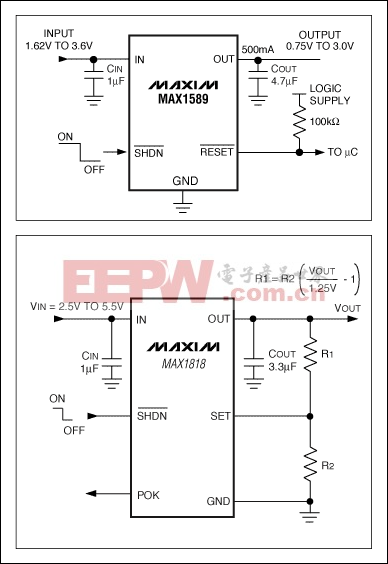
Linear regulators require that the input voltage is greater than the output voltage. The minimum required difference between the input voltage and the output voltage is called the dropout voltage. Modern linear regulators have dropout voltages much lower than those of early linear regulators, like the LM7905, and have come to be called low-dropout regulators, or LDOs. Maxim offers a wide variety of LDOs with preset positive output voltages as low as 0.75V and adjustable voltages down to 0.5V. We also offer negative LDOs with outputs from -2.5V to -5V.LDOs make regulating to a low DC voltage easy and economical. The MAX1589 LDO family is simple to use, feature preset output voltages that vary from 0.75V to 3.0V, and operate with less than 0.175V of dropout at their full 500mA of output current. The MAX1818 LDO family also offers preset output voltages from 0.75V to 3.0V, 500mA of output current, and feature adjustable output voltage down to 1.25V and a dropout voltage of only 0.12V at their full 500mA of output current.
Charge-Pump Voltage Converters
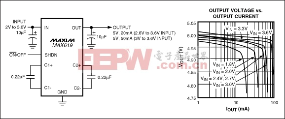
For low-current applications, the simplest solution for boosting 3V to 5V is a capacitor-based regulating charge pump (Figure 2). The industry-standard 7660 and most other charge pumps don't regulate VOUT, but the MAX619 includes an analog reference and error amplifier whose output controls a set of internal switches connected to external capacitors. The switch-capacitor network can double or triple VIN, and the MAX619 regulates by switching between these modes of operation. As indicated, this circuit produces 20mA at 5V ±4% for inputs that range between 2V and 3.6V. For inputs between 3.0V and 3.6V, the output-current capability is 50mA.Systems that handle bipolar signals usually require a negative supply, which can be generated locally if necessary. A simple solution is to use a charge-pump inverter such as the MAX889.
Inductor-Based, Switch-Mode Regulators
Switching regulators provide single or multiple outputs. Depending on the output power level, these devices are controlled by pulse-frequency modulation (PFM), pulse-width modulation (PWM), or both.. PFM control schemes, which allow high efficiency with light loads, permit the regulator to operate with quiescent supply currents as low as 10µA. PWM schemes consume more power, but they allow fixed-frequency operation for better control of noise and EMI. Some converters switch between the two control schemes based on a control signal or the load-current level.While LDOs are efficient for low values of (VIN - VOUT), many applications have an input voltage that is significantly higher than the output voltage. In this case, efficiency dictates the use of a buck-switching regulator. RF applications such as radios and cellular phones can easily use switching regulators, but care must be taken to avoid introducing noise at the sensitive IF frequencies.An ideal choice for RF applications is the MAX1684 switching regulator. This device delivers 1A at 3.3V from inputs of 4V to 12V with efficiencies up to 97%, has a 300kHz internal oscillator, and features internal MOSFETs for ease of use.An efficient buck regulator is also a good choice for upgrading an existing logic board to accommodate lower-voltage, lower-power ICs. These boards typically have 3.3V available, but they require a 1.8V supply for the new low-voltage logic. A linear regulator can easily convert 3.3V to 1.8V, but the power dissipation is prohibitive for higher load currents. At 2A, for instance, the linear regulator would dissipate 3W and require a heat-sink. The MAX1830 high-efficiency switcher (Figure 3), however, delivers 20mA to 2A with efficiencies exceeding 90% and requires no external MOSFETs, thus eliminating the need for a heat-sink.Multi-output switching regulators are intended for systems designed to operate with multiple supplies. Applications such as the generation of VCC voltages in a notebook computer, for example, are well served by the MAX1999, which generates four regulated supply voltages (Figure 4).The MAX1115, for example, converts 100k samples per second. It operates from a +3V supply using only 175µA of operating current, and uses just 1µA of current in automatic power-down mode. The MAX1115 offers a large power savings for applications in which the sampling is intermittent (Figure 5).
D/A Converters
Modern D/A converters (DACs) allow low-voltage digital systems to generate analog outputs. Intended for portable applications, these ICs require very little power and board area. The low-cost MAX5811, for instance, is a 10-bit, voltage-output DAC with low 170µA operating current and just 1µA shutdown current, which is ideal for portable applications. Its serial-data control allows it to fit into a SOT23 package.The MAX5811 operates from single 2.7V supply, and its output swings rail-to-rail. It is ideal for low-cost applications such as trimming offset voltages, setting the bias point for adjustable current (or voltage) sources, and setting the regulation point in other circuits.
Op Amps and Current Monitors
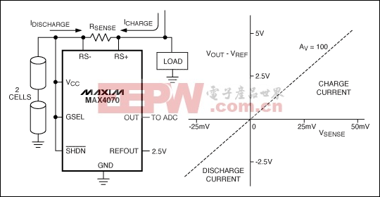
In op amps, reduced-supply operation reduces the signal-to-noise ratio (SNR) by curtailing the output-voltage swing. Many low-voltage op amps, therefore, offer rail-to-rail output swings as a means of preserving the SNR. For the same reason, many feature an input-voltage range that includes one or both supply rails.Low-voltage operation not only reduces the signal range, it puts an additional squeeze on SNR by raising the noise floor. Low-voltage amplifiers are often designed to draw low supply current, which leads to higher levels of amplifier noise. In addition, the feedback resistors have higher values (to limit system supply currents), which also adds noise.To further complicate matters, high-impedance nodes are more likely to pick up noise from high-speed digital signals through capacitive coupling. Therefore, high-impedance traces should be kept short and physically distant from high-speed digital traces.Noteworthy, and somewhat mutually exclusive, low-voltage op amp features include low supply current, low offset voltage, and high speed. The MAX4236A +3V series of devices, for example, combine a 1.7MHz gain-bandwidth product and 20µV offset voltage with a low 350µA supply current. Input common-mode voltage range is down to the negative rail, and the outputs swing rail-to-rail. These characteristics make the MAX4236A series of op amps useful as instrumentation amplifiers in low-voltage, battery-powered systems.Maxim's op amp family also features bidirectional, high-side current-sense amplifiers, such as the +2.7V MAX4069 series (Figure 6). These current-sense amplifiers minimize grounding problems by employing high-side, current-sense resistors and come in 8-/10-pin µMAX® packages.Input common-mode voltage range and output voltage swing typically become squeezed when powering op amps from low-voltage supplies. Care must be taken to observe these input and output limits when designing low-voltage circuits. Table 3 presents a cross section of data for the op amps discussed above.Table 3. A Selection of Specifications for Some of Maxim's Low-Voltage Op Amps
Part
Supply Voltage
Comparators
Like low-voltage op amps, low-voltage comparators include products separately optimized for high speed, low supply current, and low offset voltage. The MAX9100, for example, is a micropower comparator that operates from a single 1V to 5.5V supply and draws only 12µA (max) supply current. It has a 3.7ms propagation delay, 2mV offset, an output swing to within 0.3V of the supply rails, and a common-mode range that extends to the negative rail.Some applications, monitoring a power supply's output voltage for instance, require ultra-low power consumption. The MAX9017A, which operates from a 1.8V to 5.5V supply, draws only 1.2µA (typ) of supply current, and integrates a voltage reference and a comparator within a single package.
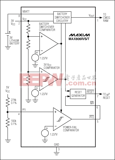
Microprocessor Supervisory Circuits
All microprocessor (µP) systems require some form of "supervision" to guard against erratic operation. The supervisor can be as simple as a reset generator, which ensures known startup conditions by issuing a system reset following the application of power. But many supervisors include other functions as well, such as backup-battery management, memory-write protection, and "watchdog" timers for monitoring software execution.Backup batteries, for example, ensure an uninterrupted flow of power to critical circuits (like the CMOS memory and the real-time clock) when VCC is absent. By monitoring VCC, the µP supervisor decides when to switch the system over to the backup battery. Low-voltage operation, however, presents an engineering problem that doesn't exist in 5V systems.Five-volt systems simply compare VCC with the backup voltage and switch to backup whenever VCC is lower. But, this approach can cause false switchovers in a lower voltage system: lithium backup batteries measure as high as 3.6V when fresh, which is higher than the 3.0V limit for VCC in a 3.3V system. Maxim's supervisors avoid this problem by allowing the backup voltage to exceed VCC, and initiating a switchover only when VCC falls below a selected threshold.The MAX823/MAX824 offers a voltage monitor and a watchdog timer in 5-pin SC70 and SOT23 packages (Figure 7).Some of Maxim's low-voltage supervisors protect the memory ICs with chip-enable (CE) gating. CE gating enables the supervisor to protect the memory by blocking read and write operations during power faults. The MAX792 and MAX820, for example, feature CE gating with a propagation delay through the supervisor of only 10ns. (Short delays allow slower, cheaper memories because the CE delay takes less of the memory cycle time.) These devices also offer manual reset, power-on reset, power-fail warning, and watchdog timing.The low-power MAX6741 monitors two system voltages, and requires only 6µA of supply current (Figure 9). All members of this supervisor family are available with either push-pull or open-drain outputs, come in the tiny SC70 package, and can monitor voltages down to 0.488V.The MAX6029 can source 4mA, and sink 1mA, with a corresponding guaranteed load regulation of 0.7µV/µA (source) and 5.5µV/µA (sink). Temperature drift is 30ppm/°C, and line regulation is typically 27µV/V over the 2.5V to 12.6V input range.
Analog Switches
Low-voltage analog switches with guaranteed precision have improved dramatically in recent years. The MAX4651/MAX4652/MAX4653 quad, 4Ω, single-pole/single-throw (SPST) analog switches operate from a single 1.8V to 5.5V supply. As expected, lower voltage operation yields somewhat higher on-resistance and moderately lower switching speeds than are available with higher-voltage supplies (Figure 11).The advent of portable and low-voltage equipment has spawned a new serial-interface specification to replace the old 232E standard, EIA/TIA-562 (562 for brevity). This new standard became effective in 1991. The 562 and 232E standards are electrically compatible, so the new 562 designs will mate with existing 232E equipment and vice versa. Despite the new standard, the term RS-232 lingers, and has come to mean both or either standard in loose parlance.A comparison of certain 232E and 562 specifications is presented in Table 4. Note that the driver output swings differ (±5V vs. ±3.7V), but the receiver input thresholds are the same (±3V). The 562 devices' ±3.7V minimum output swings allow them to communicate with 232 receivers, which have input thresholds of ±3V. The noise margin, however, is only 0.7V. By comparison, the 232 drivers' ±5V minimum swings guarantee a noise margin of 2V.Table 4. Comparison of 232E and 562 Interface Standards
Parameter
EIA-232E
EIA-562
Mode of operation
Single ended
Single ended
Allowed number of transmitters and receivers per data line
1 Tx, 1 Rx
1 Tx, 1 Rx
Maximum cable length
C 2500pF
C 2500pF for data rates 20kb/s,C 1000pF for data rates 20kb/s
Maximum data rate (kb/s)
20
64
Driver output voltage, loaded (V)
minimum
±5
±3.7
maximum
±15
±13.2
Maximum driver short-circuit current (mA)
500
60
Transmitter load impedance (kΩ)
3 to 7
3 to 7
Instantaneous slew rate (V/µs)
30
30
Receiver input threshold (sensitivity) (V)
±3
±3
Receiver input resistance (kΩ)
3 to 7
3 to 7
Receiver input range (V)
±25
±25
Figure 13. This low-voltage interface IC includes a charge pump converter that generates the voltages required for RS-232 communications.


 Systems that handle bipolar signals usually require a negative supply, which can be generated locally if necessary. A simple solution is to use a charge-pump inverter such as the MAX889.
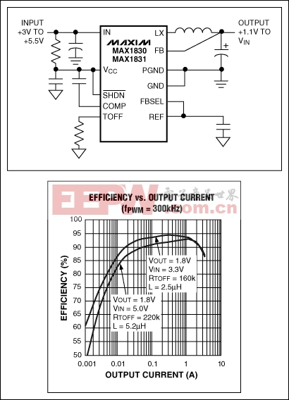 Multi-output switching regulators are intended for systems designed to operate with multiple supplies. Applications such as the generation of VCC voltages in a notebook computer, for example, are well served by the MAX1999, which generates four regulated supply voltages (Figure 4).
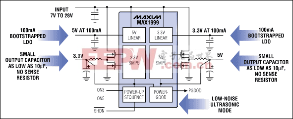 The MAX1115, for example, converts 100k samples per second. It operates from a +3V supply using only 175µA of operating current, and uses just 1µA of current in automatic power-down mode. The MAX1115 offers a large power savings for applications in which the sampling is intermittent (Figure 5).
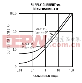
 Input common-mode voltage range and output voltage swing typically become squeezed when powering op amps from low-voltage supplies. Care must be taken to observe these input and output limits when designing low-voltage circuits. Table 3 presents a cross section of data for the op amps discussed above.Table 3. A Selection of Specifications for Some of Maxim's Low-Voltage Op Amps
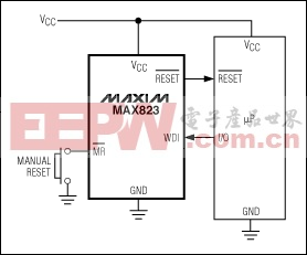
 Some of Maxim's low-voltage supervisors protect the memory ICs with chip-enable (CE) gating. CE gating enables the supervisor to protect the memory by blocking read and write operations during power faults. The MAX792 and MAX820, for example, feature CE gating with a propagation delay through the supervisor of only 10ns. (Short delays allow slower, cheaper memories because the CE delay takes less of the memory cycle time.) These devices also offer manual reset, power-on reset, power-fail warning, and watchdog timing.The low-power MAX6741 monitors two system voltages, and requires only 6µA of supply current (Figure 9). All members of this supervisor family are available with either push-pull or open-drain outputs, come in the tiny SC70 package, and can monitor voltages down to 0.488V.
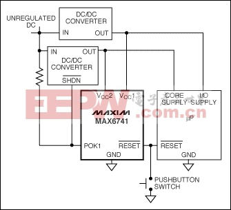 The MAX6029 can source 4mA, and sink 1mA, with a corresponding guaranteed load regulation of 0.7µV/µA (source) and 5.5µV/µA (sink). Temperature drift is 30ppm/°C, and line regulation is typically 27µV/V over the 2.5V to 12.6V input range.
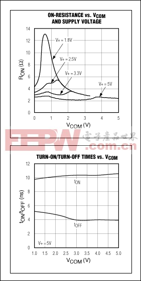
 The advent of portable and low-voltage equipment has spawned a new serial-interface specification to replace the old 232E standard, EIA/TIA-562 (562 for brevity). This new standard became effective in 1991. The 562 and 232E standards are electrically compatible, so the new 562 designs will mate with existing 232E equipment and vice versa. Despite the new standard, the term RS-232 lingers, and has come to mean both or either standard in loose parlance.A comparison of certain 232E and 562 specifications is presented in Table 4. Note that the driver output swings differ (±5V vs. ±3.7V), but the receiver input thresholds are the same (±3V). The 562 devices' ±3.7V minimum output swings allow them to communicate with 232 receivers, which have input thresholds of ±3V. The noise margin, however, is only 0.7V. By comparison, the 232 drivers' ±5V minimum swings guarantee a noise margin of 2V.Table 4. Comparison of 232E and 562 Interface Standards
评论