AD620参考设计电路|仪表放大器应用电路
AD620特性:低噪声;出色的直流性能;出色的交流特性
AD620典型应用范围:电子秤;医疗应用
AD620参考设计应用电路:

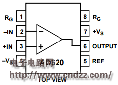
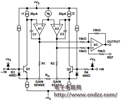
图1AD620内部结构图
TheAD620 is a low cost, high accuracy instrumentation amplifier that requires only one external resistor to set gains of 1 to 10,000. Furthermore, the AD620 features 8-lead SOIC and DIP packaging that is smaller than discrete designs and offers lower power (only 1.3 mA max supply current), making it a good fit for battery-powered, portable (or remote) applications.

图2AD620参考设计图
TheAD620 is a monolithic instrumentation amplifier based on a modification of the classic three op amp approach. Absolute value trimming allows the user to program gain accurately (to 0.15% at G = 100) with only one resistor. Monolithic construction and laser wafer trimming allow the tight matching and tracking of circuit components, thus ensuring the high level of performance inherent in this circuit.
AD620中文数据手册:点击下载
更多原理图及源代码热门应用电路:立刻点击


评论