TPS61291参考设计电路|升压转换器应用电路

TPS61291低Iq升压转换器是引脚输出电压可选且支持集成旁路模式的升压转换器。此篇主要介绍了TPS61291特性、应用范围、参考设计电路以及电路分析,帮助大家缩短设计时间。

TPS61291特性:0.9V到5V的输入电压范围;升压模式下,静态电流的典型值为5.7µA;内部反馈分压器断开连接(旁路模式);超温保护
TPS61291典型应用范围:测量(燃气表、水表、智能仪表);遥控装置;住宅安保/家庭自动化
TPS61291参考设计应用电路:
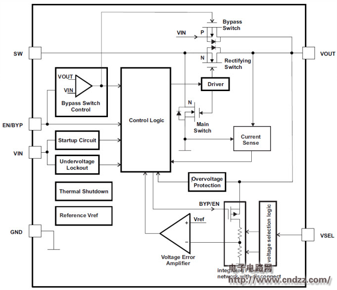
图1TPS61291内部结构图
The TPS61291 provides two operating modes: high efficiency boost mode to generate an output voltage higher than the input voltage and bypass mode, which connects the output of the device directly to the input.
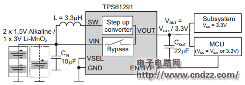
图2TPS61291参考设计图
The TPS61291 is a boost converter with pin selectable output voltages and an integrated bypass mode. In bypass operation, the device provides a direct path from the input to the system and allows a low power microcontroller (MCU) to operate directly from a single 3V Li-MnO2 battery or dual alkaline battery cells.
TPS61291中文数据手册:点击下载
更多原理图及源代码热门应用电路:立刻点击
评论