TPS54560参考设计电路|DC-DC转换器应用电路


TPS54560特性:92mΩ的高侧MOSFET;与外部时钟同步;可调节UVLO(欠压闭锁)电压和迟滞;8引脚HSOICPowerPAD封装
TPS54560典型应用范围:工业自动化与马达控制;车载附件:GPS、娱乐系统;USB专用充电端口与电池充电器;12V、24V和48V工业、汽车和通信动力系统
TPS54560参考设计应用电路:
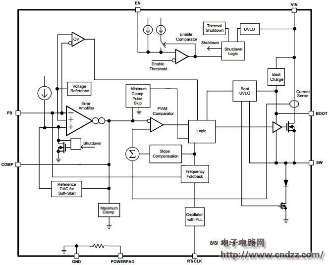
图1TPS54560内部结构图
TheTPS54560 is a 60 V, 5 A, step down regulator with an integrated high side MOSFET. The device survives load dump pulses up to 65V per ISO 7637.Current mode control provides simple external compensation and flexible component selection.
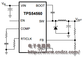
图2TPS54560参考设计图
TheTPS54560 is a 60 V, 5 A, step-down (buck) regulator with an integrated high side n-channel MOSFET. The device implements constant frequency, current mode control which reduces output capacitance and simplifies external frequency compensation. The wide switching frequency range of 100 kHz to 2500 kHz allows either efficiency or size optimization when selecting the output filter components.
TPS54560中文数据手册:点击下载
更多原理图及源代码热门应用电路:立刻点击
评论