真空荧光显示器件参考设计为汽车应用-VacuumFluorescentDisplay(VFD)ReferenceDe...

Abstract: This article describes a vacuum fluorescent display (VFD) and some ideal applications for the technology. The reference design then shows how to use a MAX15005 power-supply controller in a flyback topology to obtain multiple output voltages for a vacuum fluorescent display.
IntroductionThis reference design shows a solution for obtaining the drive voltage required for a vacuum fluorescent display (VFD) power supply in automotive applications. The design includes the complete schematic, and presents the bill of materials (BOM), load/line regulation measurements, and test results.
VFD BasicsThe VFD is composed of three basic electrodes—the cathode filaments, anodes (phosphor), and grids—under a high-vacuum condition in a glass envelope. The cathode consists of fine tungsten wires, coated by alkaline earth metal oxides which emit electrons. The grids are a thin metal mesh, which controls and diffuses electrons emitted from the cathode. The anodes are conductive electrodes src="/data/attachment/portal/201007/ET27218201007210939561.gif">
Figure 1. Schematic of the MAX15005B flyback converter for FSW = 22kHz.
The bill of materials (BOM) for this reference design is given in Table 1.
Table 1. Bill of Materials for VFD Reference Design DesignatorValueDescriptionPart NumberFootprintManufacturerQuantityC1, C11, C1210nF, 100VCapacitorC2012X7R2A103K0805TDK®3C2, C7270pF, 100VCapacitorGRM188R72A271KA01D0805Murata®2C3, C5100nF, 100VCapacitorC2012X7R2A104K0805TDK2C43.3nF, 25VCapacitor08053A332FAT2A0805AVX® Corporation1C6, C81µF, 50VCapacitorC3216X7R1H105K1206TDK2C9100pF, 100VCapacitorGRM2165C2A101JA01D0805Murata1C10330µF, 35VCapacitor–SMDTDK1C13, C14, C15, C16, C17, C182.2µF, 100VCapacitorGRM32ER72A225KA35L1210Murata6D13A, 400VDiodeS3GSMCVishay®1D2, D3, D41A, 200VDiodeES1DSMAVishay3Q111A, 55Vn-FETBUK92150-55A–NXP®1R132.4kΩResistorSMD, 5%, 0.125W0805KOA1R2, R9, R17100kΩResistorSMD, 5%, 0.125W0805KOA3R321kΩResistorSMD, 1%, 0.125W0805KOA1R4, R6100kΩResistorSMD, 1%, 0.250W1206KOA2R51.62kΩResistorSMD, 1%, 0.125W0805KOA1R71.43kΩResistorSMD, 1%, 0.125W0805KOA1R810kΩResistorSMD, 5%, 0.125W0805KOA1R10499ΩResistorSMD, 1%, 0.125W0805KOA1R11100ΩResistorSMD, 5%, 0.125W0805KOA1R121kΩResistorSMD, 1%, 0.333W1210KOA1R130.06ΩResistorSMD, 1%, SL1SL1KOA1R1433kΩResistorSMD, 5%, 0.125W0805KOA1R15, R161.0ΩResistorSMD, 1%, 0.250W1206KOA2T154µHTransformerDCT20EFD-UxxSOA5SMDTDK1Z19.1VZener diode1SMB5924BTSMBVishay1IC1MAX15005BBoost controllerMAX15005BAUE+16TSSOPMAXIM®1
Waveform MeasurementsThe following test results were generated from the board built for evaluating the circuit.
Test conditions: VIN = 14V; RANODE = 3.3kΩ; RGRID = 3.3kΩ; RFILAMENT = 8Ω.
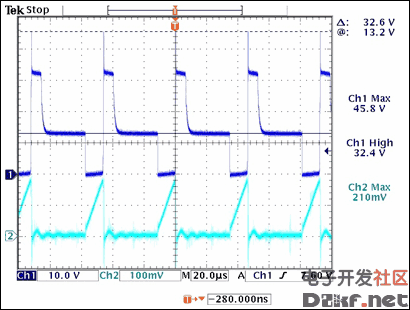
Ch1: MOSFET Q1 drain voltage (VDRAIN); Ch2: current-sense voltage across R13 (VISENSE).
Test conditions: VIN = 14V; RANODE = 3.3kΩ; RGRID = 3.3kΩ; RFILAMENT = 8Ω.
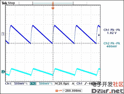
Ch1: anode output voltage ripple; Ch2: grid output voltage ripple.
Test conditions: VIN = 14V; RANODE = 3.3kΩ; RGRID = 3.3kΩ; RFILAMENT = 8Ω.
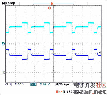
Ch1: filament positive node voltage (VF1); Ch2: filament negative node voltage (VF2).
Test conditions: VIN = 14V; RANODE = 3.3kΩ; RGRID = 3.3kΩ; RFILAMENT = 8Ω.
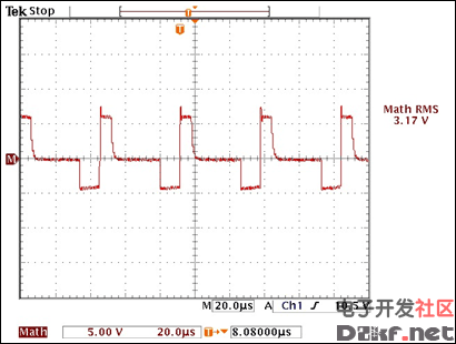
M: effective filament voltage (VF1 - VF2)
Line/Load Regulation DataThe following line/load regulation data was taken from the test board over the input voltage range and load.
VINI77 (mA)I55 (mA)V77 (VDC)V55 (VDC)VF (VRMS)9.07.75.577.055.22.417.716.777.055.02.647.744.077.054.83.0323.05.577.055.42.8223.016.777.055.22.9723.044.077.055.03.2461.65.577.055.83.3561.616.777.055.63.4361.644.077.055.43.6214.07.75.577.055.22.527.716.777.055.02.757.744.077.054.83.1423.05.577.055.42.8023.016.777.055.23.0823.044.077.055.03.3661.65.577.055.83.5061.616.777.055.73.5961.644.077.055.43.7916.07.75.577.055.22.637.716.777.055.02.867.744.077.054.83.2523.05.577.055.43.0423.016.777.055.23.2023.044.077.055.03.4961.65.577.054.83.2561.616.777.055.03.4961.644.077.055.43.92
ConclusionThis application note presents a power-supply reference design for driving a typical vacuum fluorescent display in an automotive application. The design was built to the specifications presented here. The design was then tested. The circuit schematic, BOM, and typical waveforms have been presented.

IntroductionThis reference design shows a solution for obtaining the drive voltage required for a vacuum fluorescent display (VFD) power supply in automotive applications. The design includes the complete schematic, and presents the bill of materials (BOM), load/line regulation measurements, and test results.
VFD BasicsThe VFD is composed of three basic electrodes—the cathode filaments, anodes (phosphor), and grids—under a high-vacuum condition in a glass envelope. The cathode consists of fine tungsten wires, coated by alkaline earth metal oxides which emit electrons. The grids are a thin metal mesh, which controls and diffuses electrons emitted from the cathode. The anodes are conductive electrodes src="/data/attachment/portal/201007/ET27218201007210939561.gif">
Figure 1. Schematic of the MAX15005B flyback converter for FSW = 22kHz.
The bill of materials (BOM) for this reference design is given in Table 1.
Table 1. Bill of Materials for VFD Reference Design DesignatorValueDescriptionPart NumberFootprintManufacturerQuantityC1, C11, C1210nF, 100VCapacitorC2012X7R2A103K0805TDK®3C2, C7270pF, 100VCapacitorGRM188R72A271KA01D0805Murata®2C3, C5100nF, 100VCapacitorC2012X7R2A104K0805TDK2C43.3nF, 25VCapacitor08053A332FAT2A0805AVX® Corporation1C6, C81µF, 50VCapacitorC3216X7R1H105K1206TDK2C9100pF, 100VCapacitorGRM2165C2A101JA01D0805Murata1C10330µF, 35VCapacitor–SMDTDK1C13, C14, C15, C16, C17, C182.2µF, 100VCapacitorGRM32ER72A225KA35L1210Murata6D13A, 400VDiodeS3GSMCVishay®1D2, D3, D41A, 200VDiodeES1DSMAVishay3Q111A, 55Vn-FETBUK92150-55A–NXP®1R132.4kΩResistorSMD, 5%, 0.125W0805KOA1R2, R9, R17100kΩResistorSMD, 5%, 0.125W0805KOA3R321kΩResistorSMD, 1%, 0.125W0805KOA1R4, R6100kΩResistorSMD, 1%, 0.250W1206KOA2R51.62kΩResistorSMD, 1%, 0.125W0805KOA1R71.43kΩResistorSMD, 1%, 0.125W0805KOA1R810kΩResistorSMD, 5%, 0.125W0805KOA1R10499ΩResistorSMD, 1%, 0.125W0805KOA1R11100ΩResistorSMD, 5%, 0.125W0805KOA1R121kΩResistorSMD, 1%, 0.333W1210KOA1R130.06ΩResistorSMD, 1%, SL1SL1KOA1R1433kΩResistorSMD, 5%, 0.125W0805KOA1R15, R161.0ΩResistorSMD, 1%, 0.250W1206KOA2T154µHTransformerDCT20EFD-UxxSOA5SMDTDK1Z19.1VZener diode1SMB5924BTSMBVishay1IC1MAX15005BBoost controllerMAX15005BAUE+16TSSOPMAXIM®1
Waveform MeasurementsThe following test results were generated from the board built for evaluating the circuit.
Test conditions: VIN = 14V; RANODE = 3.3kΩ; RGRID = 3.3kΩ; RFILAMENT = 8Ω.
Ch1: MOSFET Q1 drain voltage (VDRAIN); Ch2: current-sense voltage across R13 (VISENSE).
Test conditions: VIN = 14V; RANODE = 3.3kΩ; RGRID = 3.3kΩ; RFILAMENT = 8Ω.
Ch1: anode output voltage ripple; Ch2: grid output voltage ripple.
Test conditions: VIN = 14V; RANODE = 3.3kΩ; RGRID = 3.3kΩ; RFILAMENT = 8Ω.
Ch1: filament positive node voltage (VF1); Ch2: filament negative node voltage (VF2).
Test conditions: VIN = 14V; RANODE = 3.3kΩ; RGRID = 3.3kΩ; RFILAMENT = 8Ω.
M: effective filament voltage (VF1 - VF2)
Line/Load Regulation DataThe following line/load regulation data was taken from the test board over the input voltage range and load.
VINI77 (mA)I55 (mA)V77 (VDC)V55 (VDC)VF (VRMS)9.07.75.577.055.22.417.716.777.055.02.647.744.077.054.83.0323.05.577.055.42.8223.016.777.055.22.9723.044.077.055.03.2461.65.577.055.83.3561.616.777.055.63.4361.644.077.055.43.6214.07.75.577.055.22.527.716.777.055.02.757.744.077.054.83.1423.05.577.055.42.8023.016.777.055.23.0823.044.077.055.03.3661.65.577.055.83.5061.616.777.055.73.5961.644.077.055.43.7916.07.75.577.055.22.637.716.777.055.02.867.744.077.054.83.2523.05.577.055.43.0423.016.777.055.23.2023.044.077.055.03.4961.65.577.054.83.2561.616.777.055.03.4961.644.077.055.43.92
ConclusionThis application note presents a power-supply reference design for driving a typical vacuum fluorescent display in an automotive application. The design was built to the specifications presented here. The design was then tested. The circuit schematic, BOM, and typical waveforms have been presented.
AVX is a registered trademark of AVX Corporation.
Maxim is a registered trademark of Maxim Integrated Products, Inc.
Murata is a registered trademark of Murata Manufacturing Co., Ltd.
NXP is a registered trademark of NXP Semiconductors.
TDK is a registered trademark of TDK Corporation.
Vishay is a registered trademark of Vishay Intertechnology, Inc.
-- END: DB HTML --
评论
谢谢分享
谢谢分享
谢谢分享。
谢谢分享