
HowtoIncreasetheBandwidthofDigitalPotentiometers10xto100x
Abstract: A simple circuit technique is described to increase the bandwidth of digital potentiometers by a factor of 10 to 100. Using this technique can enable digital potentiometers to be used in high frequency applications at video bandwidths.
Digital potentiometers (or digital pots, or digipots) are extremely useful for controlling or adjusting circuit parameters. Normally they are src="/data/attachment/portal/201007/ET33815201007230417391.gif">
Figure 1. Typical Digital Poteniometer circuit configuration.
NOTE: With the inclusion of an op amp, the circuit can be used for gain, as well as attenuation. However, regardless of the circuit topology chosen, the method for increasing bandwidth—illustrated below—applies.
To calculate the transfer function of the circuit (VOUT/VIN), it is useful to use a different model for the potentiometer - see Figure 2. In this figure, R2 has been broken into R2top and R2bottom, where R2top is the portion of the resistance above the wiper, and R2bottom is the portion of the resistance below the wiper. Assuming we are using a pot with a 10kΩ end-to-end resistance (and neglecting the affect of wiper resistance), the ideal transfer function of R2top and R2bottom vs. digital code is as shown in Figure 3. The two end-points and the mid-point of the transfer function are useful to note: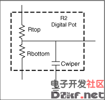
Figure 2. The digital Pot with R2 broken into R2top and R2bottom.
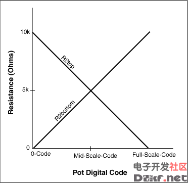
Figure 3. Digital Pot ideal transfer function.
Inspection of Figure 4 yields the dc transfer function for VOUT/VIN: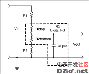
Figure 4. Typical Digital Poteniometer circuit configuration with new model for digital potentiometer.
Next, let's make some assumptions:
AssumptionsAssume R2 = 10kΩ (a common digital pot resistance value), and assume we want to attenuate the incoming signal to some arbitrary level, say 70% ±5% of its input value (i.e. from 65% to 75% of its input value).
Then using equations (1)–(4), we can see that an adjustment range of 65% to 75%, with a nominal (mid-scale setting) of 70% occurs for:
Note that the analysis in this article assumes that it is solely the wiper capacitance in parallel with the pot resistance, which sets the bandwidth. This is valid for relatively straightforward implementations of digital pots, but the bandwidth can be limited even more, if more complicated pot implementations are used. That said, however, the discussions below src="/data/attachment/portal/201007/ET33815201007230417395.gif">
Figure 5. Using src="/data/attachment/portal/201007/ET33815201007230417396.gif">
Figure 6. Using two resistors (R4 and R5) in parallel with the original circuit, to increase bandwidth 100 times over Figures 1 and 2.
Using a Parallel Resistor String to Lower the Circuit ImpedanceThe circuit of Figure 6, adds a parallel resistor string to that of Figure 1 (note the use of the model for a digital pot introduced in Figure 2). This parallel string lowers the impedance of the circuit (thus improving its bandwidth), and it also does double duty by setting the gain of the circuit and limiting the attenuation caused by the digital pot as it swings from 0-Code to Full-Scale Code.
Setting the gain of the potentiometer circuit and limiting its adjustment range by using parallel devices (R4 and R5), instead of by simply src="/data/attachment/portal/201007/ET33815201007230417397.gif" top? part of the circuit.?>
Figure 7. Simplifying the resistors in the "top" part of the circuit.
In Figure 8, the resistors in the bottom part of the circuit are combined using the equation in that figure. Note that since R5 is in parallel with R3 and R2bottom, it too lowers the circuit impedance. It is this lowered circuit impedance that gives us the dramatic bandwidth gains which we're searching for.
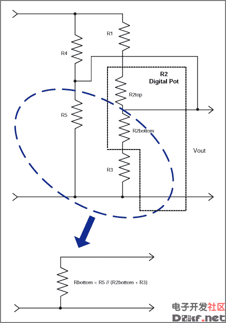
Figure 8. Simplifying the resistors in the "bottom" part of the circuit.
Figure 9 combines both simplifications from the previous figures, and gives the equations for the VOUT/VIN transfer function. It should be clear from this figure that by lowering the impedance of the circuit (Rtop is lower than R1 + R2top, Rbottom is lower impedance than R2bottom + R3), the bandwidth of the circuit has increased.
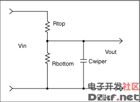
Figure 9. Circuit with the simplifications of Figures 7 and 8.
Actual ValuesBy plugging in some actual values for R1, R3, R4, and R5, we can compare the resultant bandwidth to that achieved for the circuit of Figure 1, and thus quantify the effect of R4 and R5 on the circuit performance.
Using the equations in Figure 9, we can come up with values for R1, R3, R4, and R5, and can then calculate the resultant bandwidths.
Using a spreadsheet, one can find component values that satisfy the equations in Figure 9:
Table 2. Bandwidth of the circuit of Figure 6, with Resistance Values of Equation 6. ConditionCwiper = 10pF*-0.1dB bandwidth-0.5dB bandwidth-3dB BandwidthPot at 0 Code4.1MHz9.3MHz26.3MHzPot at Mid Scale4MHz8.9MHz25.1MHzPot at Full Scale4.3MHz9.6MHz27.3MHz*Note the bandwidth scales inversely with wiper capacitance. For example, with a 3pF Cwiper, the bandwidths will be at a 3.3x higher frequency (i.e. 10/3).
SummaryThis article has shown how by simply adding a few resistors in parallel with a relatively low bandwidth digital potentiometer the resulting bandwidth can be increased by a factor of 100, a significant improvement. This assumes that the applications can tolerate the reduced control range necessary for the improvement. The increased bandwidth can enable the use of digital pots for high frequency applications, previously not considered, such as video signal path control.

Digital potentiometers (or digital pots, or digipots) are extremely useful for controlling or adjusting circuit parameters. Normally they are src="/data/attachment/portal/201007/ET33815201007230417391.gif">
Figure 1. Typical Digital Poteniometer circuit configuration.
NOTE: With the inclusion of an op amp, the circuit can be used for gain, as well as attenuation. However, regardless of the circuit topology chosen, the method for increasing bandwidth—illustrated below—applies.
To calculate the transfer function of the circuit (VOUT/VIN), it is useful to use a different model for the potentiometer - see Figure 2. In this figure, R2 has been broken into R2top and R2bottom, where R2top is the portion of the resistance above the wiper, and R2bottom is the portion of the resistance below the wiper. Assuming we are using a pot with a 10kΩ end-to-end resistance (and neglecting the affect of wiper resistance), the ideal transfer function of R2top and R2bottom vs. digital code is as shown in Figure 3. The two end-points and the mid-point of the transfer function are useful to note:
- (1) When the Pot code = 0, R2top = 10kΩ and R2bottom = 0kΩ
(2) When the Pot code = Mid-Scale, R2top = R2bottom = 5kΩ
(3) When the Pot code = Full-Scale, R2top = 0kΩ and R2bottom = 10kΩ
Figure 2. The digital Pot with R2 broken into R2top and R2bottom.
Figure 3. Digital Pot ideal transfer function.
Inspection of Figure 4 yields the dc transfer function for VOUT/VIN:
- (4) VOUT/VIN = (R3 + R2bottom)/(R1 + R2 + R3), where R2 = R2top + R2bottom
Figure 4. Typical Digital Poteniometer circuit configuration with new model for digital potentiometer.
Next, let's make some assumptions:
AssumptionsAssume R2 = 10kΩ (a common digital pot resistance value), and assume we want to attenuate the incoming signal to some arbitrary level, say 70% ±5% of its input value (i.e. from 65% to 75% of its input value).
Then using equations (1)–(4), we can see that an adjustment range of 65% to 75%, with a nominal (mid-scale setting) of 70% occurs for:
- (5) R1 = 24.9kΩ and R3 = 64.9kΩ.
Note that the analysis in this article assumes that it is solely the wiper capacitance in parallel with the pot resistance, which sets the bandwidth. This is valid for relatively straightforward implementations of digital pots, but the bandwidth can be limited even more, if more complicated pot implementations are used. That said, however, the discussions below src="/data/attachment/portal/201007/ET33815201007230417395.gif">
Figure 5. Using src="/data/attachment/portal/201007/ET33815201007230417396.gif">
Figure 6. Using two resistors (R4 and R5) in parallel with the original circuit, to increase bandwidth 100 times over Figures 1 and 2.
Using a Parallel Resistor String to Lower the Circuit ImpedanceThe circuit of Figure 6, adds a parallel resistor string to that of Figure 1 (note the use of the model for a digital pot introduced in Figure 2). This parallel string lowers the impedance of the circuit (thus improving its bandwidth), and it also does double duty by setting the gain of the circuit and limiting the attenuation caused by the digital pot as it swings from 0-Code to Full-Scale Code.
Setting the gain of the potentiometer circuit and limiting its adjustment range by using parallel devices (R4 and R5), instead of by simply src="/data/attachment/portal/201007/ET33815201007230417397.gif" top? part of the circuit.?>
Figure 7. Simplifying the resistors in the "top" part of the circuit.
In Figure 8, the resistors in the bottom part of the circuit are combined using the equation in that figure. Note that since R5 is in parallel with R3 and R2bottom, it too lowers the circuit impedance. It is this lowered circuit impedance that gives us the dramatic bandwidth gains which we're searching for.
Figure 8. Simplifying the resistors in the "bottom" part of the circuit.
Figure 9 combines both simplifications from the previous figures, and gives the equations for the VOUT/VIN transfer function. It should be clear from this figure that by lowering the impedance of the circuit (Rtop is lower than R1 + R2top, Rbottom is lower impedance than R2bottom + R3), the bandwidth of the circuit has increased.
Figure 9. Circuit with the simplifications of Figures 7 and 8.
Actual ValuesBy plugging in some actual values for R1, R3, R4, and R5, we can compare the resultant bandwidth to that achieved for the circuit of Figure 1, and thus quantify the effect of R4 and R5 on the circuit performance.
Using the equations in Figure 9, we can come up with values for R1, R3, R4, and R5, and can then calculate the resultant bandwidths.
Using a spreadsheet, one can find component values that satisfy the equations in Figure 9:
- (6) R1 = 3.48kΩ, R2 = 10kΩ, R3 = 4.53kΩ, R4 = 1kΩ, and R5 = 2.8kΩ.
Table 2. Bandwidth of the circuit of Figure 6, with Resistance Values of Equation 6. ConditionCwiper = 10pF*-0.1dB bandwidth-0.5dB bandwidth-3dB BandwidthPot at 0 Code4.1MHz9.3MHz26.3MHzPot at Mid Scale4MHz8.9MHz25.1MHzPot at Full Scale4.3MHz9.6MHz27.3MHz*Note the bandwidth scales inversely with wiper capacitance. For example, with a 3pF Cwiper, the bandwidths will be at a 3.3x higher frequency (i.e. 10/3).
SummaryThis article has shown how by simply adding a few resistors in parallel with a relatively low bandwidth digital potentiometer the resulting bandwidth can be increased by a factor of 100, a significant improvement. This assumes that the applications can tolerate the reduced control range necessary for the improvement. The increased bandwidth can enable the use of digital pots for high frequency applications, previously not considered, such as video signal path control.
SPI is a trademark of Motorola, Inc.
DS1267±5V、双路、数字电位器芯片(, 328kB)
DS1669Dallastat数字电位器(, 180kB)
DS1803可编址、双路数字电位器(, 304kB)
DS1805可编址数字电位器(, 260kB)
DS1806六路、数字电位器(, 296kB)
DS1809Dallastat(, 128kB)
DS1844四路数字电位器(, 272kB)
DS1867双路数字电位器,带有EEPROM(, 320kB)
DS1868双路、数字电位器芯片(, 284kB)
DS18693V、Dallastat数字电位器(, 144kB)
MAX5402256抽头、µPoT、低漂移数字电位器(, 224kB)
MAX5403双路、256抽头、低漂移、数字电位器,10引脚µMAX封装(, 444kB)
MAX5413双路、256抽头、低漂移、数字电位器,14引脚TSSOP封装(, 544kB)
MAX5450双路、256抽头、增/减控制接口数字电位器(, 492kB)
MAX5451双路、256抽头、增/减控制接口数字电位器(, 492kB)

评论