
单位增益缓冲器:The Unity-Gain Buffer

单位增益缓冲器:The Unity-Gain BufferThe unity-gain buffer is shown in Figure 3. The circuit gives the highest input impedance of any operational amplifier circuit. Input impedance is equal to the differential input impedance multiplied by the open-loop gain, in parallel with common mode input impedance. The gain error of this circuit is equal to the reciprocal of the amplifier open-loop gain or to the common mode rejection, whichever is less. Input impedance is a misleading concept in a DC coupled unity-gain buffer. Bias current for the amplifier will be supplied by the source resistance and will cause an error at the amplifier input due to its voltage drop across the source resistance. Since this is the case, a low bias current amplifier such as the LH1026 should be chosen as a unity-gain buffer when working from high source resistances. Bias current compensation techniques are discussed in Reference 5. The cautions to be observed in applying this circuit are three: the amplifier must be compensated for unity gain operation, the output swing of the amplifier may be limited by the amplifier common mode range, and some amplifiers exhibit a latch-up mode when the amplifier common mode range is exceeded. The LM107 may be used in this circuit with none of these problems; or, for faster operation, the LM102 may be chosen.
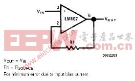
图3给出了单位增益放大器(缓冲器、跟随器——译者)的电路。这个电路在所有的放大器组态电路中具有最高的输入阻抗。其输入阻抗值为,开环增益与差模输入阻抗之积和共模输入阻抗相并联。其增益误差等于开环增益的倒数、CMRR值中较小者。在这种直流耦合,单位增益组态下,输入电阻是一个不合适的电路概念。由于输入偏置电流由信号源提供,这样就会在信号源的内阻上造成压降,成为输入信号电压的误差来源。在这种情况下,可以选用例如LH1026之类的低偏置电流的OP,以便减小在对高内阻信号源放大的情况下的误差。偏置电流补偿技术请参考文献5。本电路的设计注意事项有3个:必须对OP在单位增益状态下作补偿。输出电压的摆幅可能会被OP的共模范围所限制。在输入超过起共模范围时,有的OP可能会进入阻塞状态。LM107可以避免上述问题,另外也可以选用高速OP,LM102。
评论