复位稳定放大器:The Reset Stabilized A


复位稳定放大器:The Reset Stabilized Amplifier
The reset stabilized amplifier is a form of chopper-stabilized amplifier and is shown in Figure 23. As shown, the amplifier is operated closed-loop with a gain of one.
The connection is useful in eliminating errors due to offset voltage and bias current. The output of this circuit is a pulse whose amplitude is equal to VIN. Operation may be understood by considering the two conditions corresponding to the position of S1. When S 1 is in position 2, the amplifier is connected in the unity gain connection and the voltage at the output will be equal to the sum of the input offset voltage and the drop across R2 due to input bias current. The voltage at the inverting input will be equal to input offset voltage. Capacitor C1 will charge to the sum of input offset voltage and VIN through R1. When C1 is charged, no current flows through the source resistance and R1 so there is no error due to input resistance. S1 is then changed to position 1. The voltage stored on C1 is inserted between the output and inverting input of the amplifier and the output of the amplifier changes by VIN to maintain the amplifier input at the input offset voltage. The output then changes from (VOS + IbiasR2) to (VIN + IbiasR2) as S1 is changed from position 2 to position 1. Amplifier bias current is supplied through R2 from the output of the amplifier or from C2 when S1 is in position 2 and position 1 respectively. R3 serves to reduce the offset at the amplifier output if the amplifier must have maximum linear range or if it is desired to DC couple the amplifier.
An additional advantage of this connection is that input resistance approaches infinity as the capacitor C1 approaches full charge, eliminating errors due to loading of the source resistance. The time spent in position 2 should be long with respect to the charging time of C1 for maximum accuracy.
The amplifier used must be compensated for unity gain operation and it may be necessary to overcompensate because of the phase shift across R2 due to C1 and the amplifier input capacity. Since this connection is usually used at very low switching speeds, slew rate is not normally a practical consideration and overcompensation does not reduce accuracy.
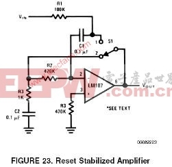
复位稳定放大器是斩波稳定放大器的一种,其电路如图23所示。在图中的状态为,放大器工作于闭环增益为1的情况。
这种电路可有效消除因失调电压和偏置电流引起的误差。该电路的输出是一个幅值等于VIN的脉冲。为了理解其工作原理,需要分析一下将开关S1拨向不同的位置时,电路结构如何改变。先将S1拨到位置2,此时放大器为单位增益接法——输出端电压等于输入失调电压加上R2与输入偏置电流产生的电压,反相端的电压等于输入失调电压,电容C1持续充电直到其端电压等于输入失调电压与VIN的代数和。C1充电完毕时,流经信号源内阻及R1的电流为零,因此信号源内阻不会造成误差。接着S1拨到位置1,使C1的电压加在放大器的输出端和反相输入端之间,(由于电容端电压不能突变,所以)输出端的电压将产生大小等于VIN的变化,使放大器输入端维持输入失调电压,即当开关S1从位置2拨到位置1时,输出端电压将从(VOS + IbiasR2)变为(VIN + IbiasR2)。S1处于位置2时,放大器的偏置电流是由输出端经电阻R2提供的,当S1转向位置1时则由C2提供。R3的作用是降低输出失调电压,如果要求放大器具有最大的线性范围,或者采用直流耦合,就应该使用该电容。
上面这个电路的另一个优点在于,当电容C1充电完毕后,输入电阻将趋于无穷大,因此可以消除因信号源内阻产生的误差。开关接通位置2的持续时间要足够长,以保证电容C1完成充电,这样才能获得最佳的精度。
此电路必须使用单位增益稳定的OP,因为R2—C1产生的相移,所以还可能需要一定的过补偿。鉴于本电路常用于切换频率很低的场合,转换速率(SR)一般不是关键指标,因此过补偿不会降低精度。
评论