
模拟乘法器:The Analog Multiplier

模拟乘法器:The Analog MultiplierA simple embodiment of the analog multiplier is shown in Figure 24. This circuit circumvents many of the problems associated with the log-antilog circuit and provides three quadrant analog multiplication which is relatively temperature insensitive and which is not subject to the bias current errors which plague most multipliers.
Circuit operation may be understood by considering A2 as a controlled gain amplifier, amplifying V2, whose gain is dependent on the ratio of the resistance of PC2 to R5 and by considering A1 as a control amplifier which establishes the resistance of PC2 as a function of V 1. In this way it is seen that VOUT is a function of both V1 and V2.
A1, the control amplifier, provides drive for the lamp, L1. When an input voltage, V1, is present, L1 is driven by A1 until the current to the summing junction from the negative supply through PC1 is equal to the current to the summing junction from V1 through R1. Since the negative supply voltage is fixed, this forces the resistance of PC1 to a value proportional to R1 and to the ratio of V1 to V -. L1 also illuminates PC2 and, if the photoconductors are matched, causes PC2 to have a resistance equal to PC1.
A2, the controlled gain amplifier, acts as an inverting amplifier whose gain is equal to the ratio of the resistance of PC2 to R5. If R5 is chosen equal to the product of R1 and V-, then VOUT becomes simply the product of V1 and V2. R5 may be scaled in powers of ten to provide any required output scale factor.
PC1 and PC2 should be matched for best tracking over temperature since the T.C. of resistance is related to resistance match for cells of the same geometry. Small mismatches may be compensated by varying the value of R5 as a scale factor adjustment. The photoconductive cells should receive equal illumination from L1, a convenient method is to mount the cells in holes in an aluminum block and to mount the lamp midway between them. This mounting method provides controlled spacing and also provides a thermal bridge between the two cells to reduce differences in cell temperature. This technique may be extended to the use of FET’s or other devices to meet special resistance or environment requirements.
The circuit as shown gives an inverting output whose magnitude is equal to one-tenth the product of the two analog inputs. Input V 1 is restricted to positive values, but V2 may assume both positive and negative values. This circuit is restricted to low frequency operation by the lamp time constant.
R2 and R4 are chosen to minimize errors due to input offset current as outlined in the section describing the photocell amplifier. R3 is included to reduce in-rush current when first turning on the lamp, L1.
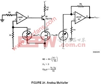
图24给出了一个简单的模拟乘法器电路。这个电路不但克服了对数-反对数方式实现乘法的缺陷,而且可以实现不受温度变化影响的3象限乘法运算。绝大多数的乘法器都存在偏置电流误差的困扰,本电路解决了这个问题。
为便于理解本电路的原理,可以将A2视为一个增益受A1控制的放大器,A1在PC2的阻值与V1之间建立起函数关系,A2对V2进行放大,其增益由PC2和R5的阻值之比决定。因此,VOUT是V1和V2的函数。
控制方放大器A1,驱动灯泡L1。输入电压V1时,A1输出升高,使L1逐渐变亮。当求和节点上,经PC1流回负电源的电流与V1经R1流入求和节点的电流相等时,L1亮度不再变化。因为负电源电压恒定,所以PC1的电阻等于-R1V-/V1。L1发出的光同时照射PC2,如果两个光敏电阻参数匹配,那么PC2的阻值就会等于PC1。
受控方放大器A2相当于一个增益受控制的反相放大器,其增益为-R5/PC2。如果让R5的阻值等于R1V-,那么VOUT就等于V1V2。R5的阻值是乘法运算的比例系数,可以任意设定以实现任意大小的输出,比如设置为10的幂。
PC1和PC2的温度特性应该匹配,这就要求其具有相同的几何尺寸,以保证其T.C.特性。在失配程度比较小时,可以通过改变R5的大小进行补偿。L1照射到两个光敏电阻上的光强度应该相等,有一个简便的方法可以实现这个要求,将两个光敏电阻固定在同一个铝块上的两个小孔内,灯泡则固定在两个光敏电阻的中间。采用这个方法,光敏电阻与灯泡的间距是可调的,另外,铝块在两个光敏电阻之间起了平衡温度的作用,使得其温度差减小。这个方法也可以推广到FET对管或者其他需要性能匹配的场合,满足电阻或者环境方面的特殊要求。
图示电路的输出等于两个输入电压的乘积除以10,相位相反。输入电压V1必须大于零,V2既可以为正也可以为负。受灯泡的时间常数限制,本电路只能低频工作。
R2和R4用来降低因输入失调电流产生的误差,其原理与前文光电二极管放大器所述一致。R3用于抑制灯泡L1初次通电时的浪涌电流。
评论