
正弦波振荡器:Sine Wave Oscillator

正弦波振荡器:Sine Wave Oscillator
An amplitude-stabilized sine-wave oscillator is shown in Figure 26. This circuit provides high purity sine-wave output down to low frequencies with minimum circuit complexity. An important advantage of this circuit is that the traditional tungsten filament lamp amplitude regulator is eliminated along with its time constant and linearity problems.
In addition, the reliability problems associated with a lamp are eliminated.
The Wien Bridge oscillator is widely used and takes advantage of the fact that the phase of the voltage across the parallel branch of a series and a parallel RC network connected in series, is the same as the phase of the applied voltage across the two networks at one particular frequency and that the phase lags with increasing frequency and leads with decreasing frequency. When this network—the Wien Bridge—is used as a positive feedback element around an amplifier, oscillation occurs at the frequency at which the phase shift is zero. Additional negative feedback is provided to set loop gain to unity at the oscillation frequency, to stabilize the frequency of oscillation, and to reduce harmonic distortion.
The circuit presented here differs from the classic usage only in the form of the negative feedback stabilization scheme. Circuit operation is as follows: negative peaks in excess of -8.25V cause D1 and D2 to conduct, charging C4. The charge stored in C4 provides bias to Q1, which determines amplifier gain. C3 is a low frequency roll-off capacitor in the feedback network and prevents offset voltage and offset current errors from being multiplied by amplifier gain.
Distortion is determined by amplifier open-loop gain and by the response time of the negative feedback loop filter, R5 and C4. A trade-off is necessary in determining amplitude stabilization time constant and oscillator distortion. R4 is chosen to adjust the negative feedback loop so that the FET is operated at a small negative gate bias. The circuit shown provides optimum values for a general purpose oscillator.
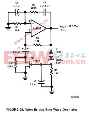
图26给出了一个带稳幅功能的正弦波振荡器。这个电路以最简洁的结构实现了高纯净度正弦波输出,而且在较低的频率上也是如此。这个电路的主要优点之一是克服了传统钨丝灯幅值调节电路所带来的时间常数以及线性度方面的问题。
此外,灯泡的可靠性问题也无需再考虑了。
文氏桥振荡器一直都被广泛地应用着,该电路的原理是——如果将一个串联RC网络和一个并联RC网络串接起来,那么在某个特定频率下,电路输出电压的相位将与输入电压的相位相等,而当频率升高时,输出电压相位滞后,当频率降低时,输出电压相位超前。这个电路就是“文氏桥”,如果以文氏桥作为放大器的正反馈路径,那么当相移等于0的时候,就会出现振荡。为了使振荡频率稳定并降低谐波失真,需要加入一个在震荡频率处能够提供单位增益的负反馈路径。
本电路与经典电路的唯一区别在于负反馈稳定部分。电路原理如下:超出-8.25V的负电平使D1和D2导通,给C4充电,C4储存的电荷为Q1提供偏置,从而控制放大器的增益。C3在反馈电路中起低通滤波的作用,防止失调电压和失调电流引起的误差被放大到输出端。
失真是开环增益和负反馈路径中滤波器的时间常数R5C4造成的。设计者需要在稳幅时间常数和振荡器的失真度之间进行权衡。R4用来调整负反馈路径,使FET工作在微小的门极反相偏置电压下。对于一般性应用,图26电路中的参数可以提供最佳性能。

评论