
NXP PC408x 32位ARM Cortex-M4 MCU开发方案

NXP公司的PC408x/7x系列是32位ARM Cortex-M4 MCU,集成多达512KB闪存,96KB SRAM,USB器件/主/OTG,以太网,LCD,EMC和SPIFI,具有低功耗,增强调试特性和支持高级区块,工作频率高达120MHz,支持单周期数字信号处理和SIMD指令,主要用于需要高度集成和低功耗的嵌入式应用如POS终端,网络服务器和多协议桥等通信领域,自动化控制器,应用控制和机器人控制,HVAC,PLS,逆变器等工业应用,音频,MP3译码器,打印机,扫描仪,健身设备等消费类电子以及后市场应用,汽车告警,GPS等汽车电子领域.本文介绍了LPC408x/7x系列特性和优势,框图,几种USB OTG应用电路,评估板RDB4078主要特性和电路图.
The LPC408x/7x is an ARM Cortex-M4 based digital signal controller for embeddedapplications requiring a high level of integration and low power dissipation.
The ARM Cortex-M4 is a next generation core that offers system enhancements such as low power consumption, enhanced debug features, and a high level of support blockintegration. The ARM Cortex-M4 CPU incorporates a 3-stage pipeline, uses a Harvardarchitecture with separate local instruction and data buses as well as a third bus forperipherals, and includes an internal prefetch unit that supports speculative branching.
The ARM Cortex-M4 supports single-cycle digital signal processing and SIMDinstructions. A hardware floating-point processor is integrated in the core for severalversions of the part.
The LPC408x/7x adds a specialized flash memory accelerator to accomplish optimalperformance when executing code from flash. The LPC408x/7x is targeted to operate atup to 120 MHz CPU frequency.
The peripheral complement of the LPC408x/7x includes up to 512 kB of flash programmemory, up to 96 kB of SRAM data memory, up to 4032 byte of EEPROM data memory,External Memory controller (EMC), LCD, Ethernet, USB Device/Host/OTG, an SPI FlashInterface (SPIFI), a General Purpose DMA controller, five UARTs, three SSP controllers,three I2C-bus interfaces, a Quadrature Encoder Interface, four general purpose timers,two general purpose PWMs with six outputs each and one motor control PWM, anultra-low power RTC with separate battery supply and event recorder, a windowedwatchdog timer, a CRC calculation engine and up to 165 general purpose I/O pins.The analog peripherals include one eight-channel 12-bit ADC, two analog comparators,and a DAC.
The pinout of LPC408x/7x is intended to allow pin function compatibility with theLPC24xx/23xx as well as the LPC178x/7x families.
LPC408x/7x系列特性和优势:
Functional replacement for LPC23xx/24xx and LPC178x/7x family devices.
ARM Cortex-M4 core:
ARM Cortex-M4 processor, running at frequencies of up to 120 MHz.
ARM Cortex-M4 built-in Memory Protection Unit (MPU) supporting eight regions.
ARM Cortex-M4 built-in Nested Vectored Interrupt Controller (NVIC).
Hardware floating-point unit (not all versions).
Non-maskable Interrupt (NMI) input.
JTAG and Serial Wire Debug (SWD), serial trace, eight breakpoints, and four watchpoints.
System tick timer.
System:
Multilayer AHB matrix interconnect provides a separate bus for each AHB master.AHB masters include the CPU, and General Purpose DMA controller. Thisinterconnect provides communication with no arbitration delays unless two mastersattempt to access the same slave at the same time.
Split APB bus allows for higher throughput with fewer stalls between the CPU andDMA. A single level of write buffering allows the CPU to continue without waiting forcompletion of APB writes if the APB was not already busy.
Embedded Trace Macrocell (ETM) module supports real-time trace.
Boundary scan for simplified board testing.
Memory:
512 kB on-chip flash program memory with In-System Programming (ISP) andIn-Application Programming (IAP) capabilities. The combination of an enhancedflash memory accelerator and location of the flash memory on the CPU localcode/data bus provides high code performance from flash.
Up to 96 kB on-chip SRAM includes:
64 kB of main SRAM on the CPU with local code/data bus for high-performanceCPU access.
Two 16 kB peripheral SRAM blocks with separate access paths for higherthroughput. These SRAM blocks may be used for DMA memory as well as forgeneral purpose instruction and data storage.
Up to 4032 byte on-chip EEPROM.
LCD controller, supporting both Super-Twisted Nematic (STN) and Thin-FilmTransistors (TFT) displays.
Dedicated DMA controller.
Selectable display resolution (up to 1024 x768 pixels).
Supports up to 24-bit true-color mode.
External Memory Controller (EMC) provides support for asynchronous static memorydevices such as RAM, ROM and flash, as well as dynamic memories such as singledata rate SDRAM.
Eight channel General Purpose DMA controller (GPDMA) on the AHB multilayermatrix that can be used with the SSP, I2S, UART, CRC engine, Analog-to-Digital andDigital-to-Analog converter peripherals, timer match signals, GPIO, and formemory-to-memory transfers.
Serial interfaces:
Quad SPI Flash Interface (SPIFI) with four lanes and up to 40 MB per second.
Ethernet MAC with MII/RMII interface and associated DMA controller. Thesefunctions reside on an independent AHB.
USB 2.0 full-speed dual port device/host/OTG controller with on-chip PHY andassociated DMA controller.
Five UARTs with fractional baud rate generation, internal FIFO, DMA support, andRS-485/EIA-485 support. One UART (UART1) has full modem control I/O, and oneUART (USART4) supports IrDA, synchronous mode, and a smart card modeconforming to ISO7816-3.
Three SSP controllers with FIFO and multi-protocol capabilities. The SSPinterfaces can be used with the GPDMA controller.
Three enhanced I2C-bus interfaces, one with a true open-drain output supportingthe full I2C-bus specification and Fast-mode Plus with data rates of 1 Mbit/s, twowith standard port pins. Enhancements include multiple address recognition andmonitor mode.
I2S (Inter-IC Sound) interface for digital audio input or output. It can be used withthe GPDMA.
CAN controller with two channels.
Digital peripherals:
SD/MMC memory card interface.
Up to 165 General Purpose I/O (GPIO) pins depending on the packaging, withconfigurable pull-up/down resistors, open-drain mode, and repeater mode. AllGPIOs are located on an AHB bus for fast access and support Cortex-M4bit-banding. GPIOs can be accessed by the General Purpose DMA Controller. Anypin of ports 0 and 2 can be used to generate an interrupt.
Two external interrupt inputs configurable as edge/level sensitive. All pins on port 0and port 2 can be used as edge sensitive interrupt sources.
Four general purpose timers/counters, with a total of eight capture inputs and tencompare outputs. Each timer block has an external count input. Specific timerevents can be selected to generate DMA requests.
Quadrature encoder interface that can monitor one external quadrature encoder.
Two standard PWM/timer blocks with external count input option.
One motor control PWM with support for three-phase motor control.
Real-Time Clock (RTC) with a separate power domain. The RTC is clocked by adedicated RTC oscillator. The RTC block includes 20 bytes of battery-poweredbackup registers, allowing system status to be stored when the rest of the chip ispowered off. Battery power can be supplied from a standard 3 V lithium button cell.The RTC will continue working when the battery voltage drops to as low as 2.1 V.An RTC interrupt can wake up the CPU from any reduced power mode.
Event Recorder that can capture the clock value when an event occurs on any ofthree inputs. The event identification and the time it occurred are stored inregisters. The Event Recorder is located in the RTC power domain and cantherefore operate as long as there is RTC power.
Windowed Watchdog Timer (WWDT). Windowed operation, dedicated internaloscillator, watchdog warning interrupt, and safety features.
CRC Engine block can calculate a CRC on supplied data using one of threestandard polynomials. The CRC engine can be used in conjunction with the DMAcontroller to generate a CRC without CPU involvement in the data transfer.
Analog peripherals:
12-bit Analog-to-Digital Converter (ADC) with input multiplexing among eight pins,conversion rates up to 400 kHz, and multiple result registers. The 12-bit ADC canbe used with the GPDMA controller.
10-bit Digital-to-Analog Converter (DAC) with dedicated conversion timer and DMAsupport.
Two analog comparators.
Power control:
Four reduced power modes: Sleep, Deep-sleep, Power-down, and Deeppower-down.
The Wake-up Interrupt Controller (WIC) allows the CPU to automatically wake upfrom any priority interrupt that can occur while the clocks are stopped inDeep-sleep, Power-down, and Deep power-down modes.
Processor wake-up from Power-down mode via any interrupt able to operateduring Power-down mode (includes external interrupts, RTC interrupt, PORT0/2pin interrupt, and NMI).
Brownout detect with separate threshold for interrupt and forced reset.
On-chip Power-On Reset (POR).
Clock generation:
Clock output function that can reflect the main oscillator clock, IRC clock, RTCclock, CPU clock, USB clock, or the watchdog timer clock.
On-chip crystal oscillator with an operating range of 1 MHz to 25 MHz.
12 MHz Internal RC oscillator (IRC) trimmed to 1 % accuracy that can optionally beused as a system clock.
An on-chip PLL allows CPU operation up to the maximum CPU rate without theneed for a high-frequency crystal. May be run from the main oscillator or theinternal RC oscillator.
A second, dedicated PLL may be used for USB interface in order to allow addedflexibility for the Main PLL settings.
Versatile pin function selection feature allows many possibilities for using on-chipperipheral functions.
Unique device serial number for identification purposes.
Single 3.3 V power supply (2.4 V to 3.6 V). Temperature range of 40 C to 85 C.
Available as LQFP208, TFBGA208, TFBGA180, LQFP144, TFBGA80, and LQFP80package.
LPC408x/7x系列应用:
Communications:
Point-of-sale terminals, web servers, multi-protocol bridges
Industrial/Medical:
Automation controllers, application control, robotics control, HVAC, PLC, inverters,circuit breakers, medical scanning, security monitoring, motor drive, video intercom
Consumer/Appliance:
Audio, MP3 decoders, alarm systems, displays, printers, scanners, smallappliances, fitness equipment
Automotive:
After-market, car alarms, GPS/fleet monitors

图1.LPC408x/7x系列框图

图2.LPC408x/7x系列USB OTG端口配置图:端口1 OTG双器件,端口2主器件

图3.LPC408x/7x系列USB OTG端口配置图:VP_VM模式

图4.LPC408x/7x系列USB 主端口配置图:端口1 和端口2主器件
图5.LPC408x/7x系列USB 器件端口配置图:端口1 和端口2器件
评估板RDB4078
The RDB4078 is a versatile platform for evaluating and developing with NXP’s LPC40xx series microcontrollers.
评估板RDB4078主要特性:
The board is fitted with an NLPC4078 microcontroller, featuring:
120 MHz ARM® Cortex-M4 with floating point in hardware and DSP extensions
512 KB Flash, 96 KB SRAM, and 4032 bytes of EEPROM
On-board debug connection suitable for use with LPCXpresso IDE or other third party tool chains without need for an additional debug probe.
A 20-pin 0.05" JTAG/SWD/ETM connector for use with external debug probe is also provided.

图6.评估板RDB4078外形图
评估板RDB4078主要特性:
2.4” 320 x 240 IPS (In Plane Switching) color LCD providing amazingly wide viewing angle
Resistive touchscreen
Wolfson high quality stereo audio codec WM8903, amplifier, on-board speaker and 3.5 mm headphone socket
Dual on-board digital microphones (WM7220) enabling spatial audio positioning applications
Standard 3.5 mm audio jacks for line level and microphone input
10/100 Mbps Ethernet port using SMSC LAN8720 PHY
High speed USB device and host connectors
Micro-SD Card interface
Serial port on standard 9-pin D-type with RS232 levels
Mini-joystick, potentiometer, plus INT and RESET buttons, for user input
4 User LEDs
CymbetEnerChip Battery Backup
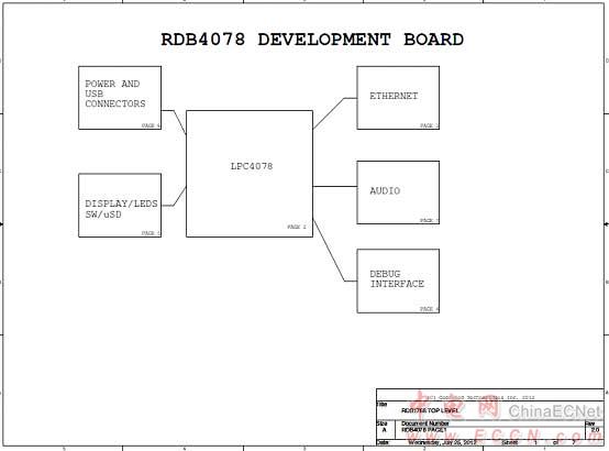
图7.评估板RDB4078电路图(1)

图8.评估板RDB4078电路图(2)

图9.评估板RDB4078电路图(3)

图10.评估板RDB4078电路图(4)
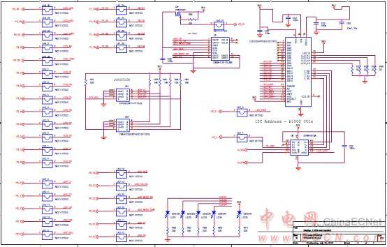
图11.评估板RDB4078电路图(5)

图12.评估板RDB4078电路图(6)
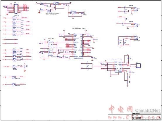
图13.评估板RDB4078电路图(7)
评论