Altera MAX 10 FPGA开发方案


Altera公司的MAX 10器件是单片非易失低成本可编逻辑器件(PLD),具有内部存储可配置的双闪存,用户闪存,集成了ADC,支持单片Nios II软件处理器,主要用在系统管理,I/O扩展,通信控制面板,汽车电子,工业控制和消费类电子产品.本文介绍了Altera® MAX® 10 FPGA主要优势,Altera® MAX® 10 FPGA开发套件主要特性,框图,元件分布图,电路图和主要元件表.
MAX® 10 devices are single-chip, non-volatile low-cost programmable logic devices (PLDs) to integrate the optimal set of system components.
The highlights of the MAX® 10 devices include:
Internally stored dual configuration flash
User flash memory
Instant on support
Integrated analog-to-digital converters (ADCs)
Single-chipNios II soft core processor support
MAX® 10 devices are the ideal solution for system management, I/O expansion, communication control planes, industrial, automotive, and consumer applications.
Altera® MAX® 10 FPGA主要优势: | |
Advantage | Supporting Feature |
Simple and fast configuration | Secure on-die flash memory enables device configuration in less than 10 ms |
Flexibility and integration | Single device integrating PLD logic, RAM, flash memory, digital signal processing (DSP), ADC, phase-locked loop (PLL), and I/Os Small packages available from 3 mm × 3 mm |
Low power | Sleep mode—significant standby power reduction and resumption in less than 1 ms Longer battery life—resumption from full power-off in less than 10 ms |
20-year-estimated life cycle | Built on TSMC’s 55 nm embedded flash process technology |
High productivity design tools | Quartus® II web edition (no cost license) Qsys system integration tool Digital Signal Processing (DSP) Builder Nios® II Embedded Design Suite (EDS) |
Altera® MAX® 10 FPGA开发套件
The Altera® MAX® 10 FPGA Development Kit provides a full featured design platform built around a 50 K logic elements (LEs) MAX 10 FPGA, optimized for system level integration with on-die analog-to-digital converter (ADC), dual-configuration flash, and DDR3 memory interface support. The board features on-board USB-BlasterTM II, high-speed mezannine card (HSMC), and Pmod™ Compatible expansion cards, high-definition multimedia interface (HDMI) output, and dual Ethernet for industrial Ethernet applications. The MAX 10 FPGA Development Kit provides the perfect system-level prototyping solution for industrial, automotive, consumer, and many other market applications.
With this development board, you can:
Develop designs for the 10M50D, F484 package FPGA
Measure the performance of the MAX 10 FPGA analog-to-digital block conversion
Interface MAX 10 FPGAs to DDR3 memory at 300 MHz performance
Run embedded Linux using the Nios® II processor
Interface to daughtercards and peripherals using HSMC and DigilentPmod™ Compatible connectors
Measure FPGA power (VCC_CORE and VCC_IO) using the power monitor graphical user interface (GUI)
Reuse the kit’s PCB board and schematic as a model for your design
The MAX 10 FPGA Development Kit includes the following:
RoHS- and CE-compliant MAX 10 FPGA development board
Featured devices
MAX 10 FPGA (10M50D, dual supply, F484 package)
Enpirion® EN2342QI 4A PowerSoC voltage-mode synchronous step-down converter with integrated inductor
Enpirion EN6337QA 3A high-efficiency PowerSoC DC-DC step-down converters with integrated inductor
Enpirion EP5358xUI 600 mA PowerSoC DC-DC step-down converters with integrated inductor
MAX II CPLD – EPM1270M256C4N (On-board USB-Blaster II)
Programming and Configuration
Embedded USB-Blaster II (JTAG)
Optional JTAG direct via 10-pin header
Memory devices
64Mx16 1 Gb DDR3 SDRAM with soft memory controller
128Mx8 1 Gb DDR3 SDRAM with soft memory controller
512Mb quad serial peripheral interface (quad SPI) flash memory
Communication ports
Two Gigabit Ethernet (GbE) RJ-45 ports
One mini-USB2.0 UART
One HDMI video output
One universal HSMC connector (see HSMC expansion cards)
Two 12-pin DigilentPmod™ Compatible connectors (see Pmod™ Compatible expansion cards)
Analog
Two MAX 10 FPGA ADC SMA inputs
2x10 ADC header
Potentiometer input to ADC
One external 16 bit digital-to-analog converter (DAC) device with SMA output
Clocking
25 MHz single-ended, external oscillator clock source
Silicon labs clock generator with programmable frequency GUI
Switches, push buttons, jumpers, and status LEDs
Mini-USB cable for on-board USB-Blaster II
2A power supply and cord
Free Quartus® II Web Edition design software (download software and license from the website)
Complete documentation
User manual, bill of materials, schematic, and board files

图1.Altera® MAX® 10 FPGA开发板主要元件分布图(正面)

图2.Altera® MAX® 10 FPGA开发板主要元件分布图(背面)

图3.Altera® MAX® 10 FPGA开发板系统框图
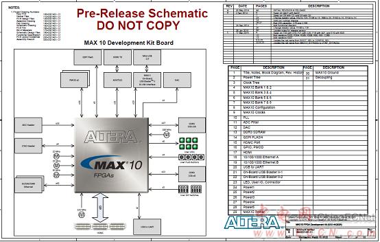
图4.Altera® MAX® 10 FPGA开发板电路图(1)

图5.Altera® MAX® 10 FPGA开发板电路图(2)
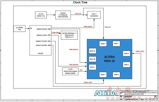
图6.Altera® MAX® 10 FPGA开发板电路图(3)

图7.Altera® MAX® 10 FPGA开发板电路图(4)
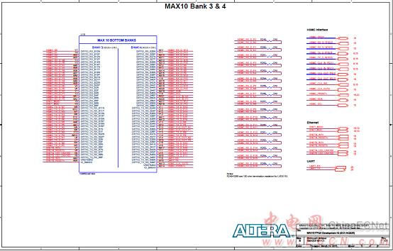
图8.Altera® MAX® 10 FPGA开发板电路图(5)

图9.Altera® MAX® 10 FPGA开发板电路图(6)
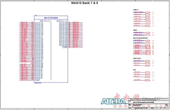
图10.Altera® MAX® 10 FPGA开发板电路图(7)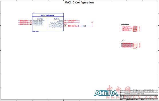
图11.Altera® MAX® 10 FPGA开发板电路图(8)

图12.Altera® MAX® 10 FPGA开发板电路图(9)
评论