利用DS1841对数电阻优化雪崩光电二极管(APD)的偏置范围分析


下面是 [利用DS1841对数电阻优化雪崩光电二极管(APD)的偏置范围分析]的电路图
(责任编辑:admin)
本文阐述了如何使用DS1841对数电位器调节APD偏置电路的输出范围。为了使调节过程更简单,本文还提供了电子数据表。
APD偏置电路
DS1841可受温度控制的非易失(NV)、I²C对数电位器包含了一个7位对数变化的电阻器。通过与升压型DC-DC转换器相配合,DS1841能够调节施加在雪崩光电二极管的偏置电压。利用三个外部电阻(RSER、RTOP和RPAR)调节输出范围(图1)。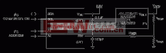
图1. 利用DS1841和升压型DC-DC转换器(此处为MAX5026或MAX1523)构成的APD偏置电路
调节APD偏置电压范围
利用电子数据表DS1841 APD偏置电压调节(xls)可以方便地调节APD偏置电压。该电子数据表包含四个输入变量:RTOP、RSER、RPAR以及VFB。输入这些电阻值后,电子数据表即可计算出四个输出值:VAPD (最大值)、VAPD (最小值)、STEP (最大值)和STEP (平均值)。此外还生成了两个曲线图:APD偏置与DAC码关系曲线和每级电压与DAC码的关系曲线图。图2所示界面给出了四个变量以及通过输入值而生成的图形。表1定义了电子数据表所使用的参数。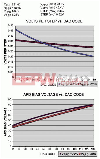
图2. 该电子数据表界面包含了四个数据输入变量(见左上角)
表1. 使用DS1841调节APD偏置电压范围时的变量定义
| VFB | The voltage present at the feedback node of the DC-DC converter. |
| VAPD (max) | The maximum voltage to which the APD bias can be set under worst-case conditions. |
| VAPD (min) | The minimum voltage to which the APD bias can be set under worst-case conditions. |
| STEP (max) | The maximum calculated voltage step that can occur between two adjacent DAC codes. |
| STEP (avg) | The average voltage step size that occurs across the full range. |
| VSTEP +20% | The voltage step size when the variable resistor is at the maximum of the process range (+20%). |
| VSTEP -20% | The voltage step size when the variable resistor is at the minimum of the process range (-20%). |
| VAPD +20% | The APD bias voltage when the variable resistor is at the maximum of the process range (+20%). |
| VAPD -20% | The APD bias voltage when the variable resistor is at the minimum of the process range (-20%). |
评论