
CY4638 WirelessUSB LP VoIP应用电路

CY7C603xx系列是低压enCoRe III PSoC器件,采用功能强大的哈佛架构,M8C处理器的速度高达12MHz,工作电压2.4V-3.6V,具有可配置的外设如8位定时器,计数器和PWM,全双工主或从SPI,10位ADC,8位SAR ADC和比较器,闪存程序存储器,SRAM数据存储器和可配置的I/O口,主要用在无线鼠标,无线游戏手柄, PlayStation® 2有线游戏手柄以及各种低压8位MCU应用.
CY7C603xx 应用:
■ Wireless mice
■ Wireless gamepads
■ Wireless presenter tools
■ Wireless keypads
■ PlayStation® 2 wired gamepads
■ PlayStation 2 bridges for wireless gamepads
Applications requiring a cost effective low voltage 8-bit microcontroller.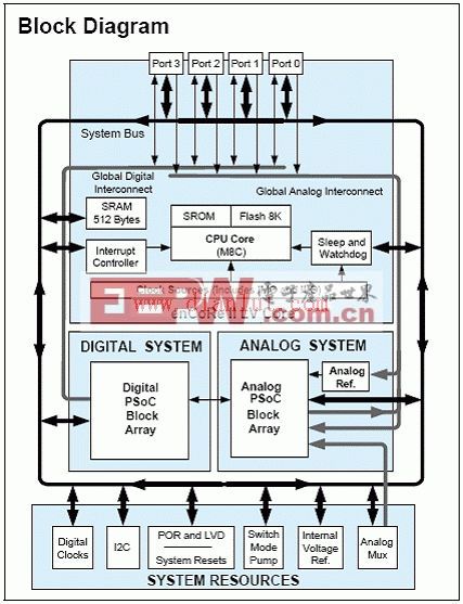
图1.CY7C603xx方框图
This architecture enables the user to create customized peripheral configurations that match the requirements of each individual application. A fast CPU, Flash program memory, SRAM data memory, and configurable IO are included in both 28-pin SSOP and 32-pin QFN packages.
The enCoRe III LV architecture consists of four main areas: the enCoRe III LV Core, the System Resources, Digital System, and Analog System. Configurable global bus resources allow combining all the device resources into a complete custom system. Each enCoRe III LV device supports a limited set of digital and analog peripherals.
Depending on the package, up to 28 general purpose IOs (GPIOs) are also included. The GPIOs provide access to the global digital and analog interconnects.
enCoRe III LV Core
The enCoRe III LV core is a powerful engine that supports a rich feature set. It encompasses SRAM for data storage, an interrupt controller, sleep and watchdog timers, and IMO (internal main oscillator) and ILO (internal low-speed oscillator).
The CPU core, called the M8C, is a powerful processor with speeds up to 12 MHz. The M8C is a four MIPS 8-bit Harvard architecture microprocessor. The core includes a CPU, memory, clocks, and configurable GPIO (General Purpose IO).
System Resources provide additional capability, such as digital clocks to increase flexibility, I2C functionality for implementing an I2C master, slave, multi-master, an internal voltage reference that provides an absolute value of 1.3V to a number of subsystems, a switch mode pump (SMP) that generates normal operating voltages off a single battery cell, and various system resets supported by the M8C.
The Digital System
The digital system consists of 4 digital enCoRe III LV blocks. Each block is an 8-bit resource. Digital peripheral configurations include the following:
■ PWM usable as timer or counter
■ SPI master and slave
■ I2C slave and multi-master
■ CMP
■ ADC10
■ SARADC
The digital blocks may be connected to any GPIO through a series of global buses that can route any signal to any pin. The buses also allow for signal multiplexing and for performing logic operations. This configurability frees your designs from the constraints of a fixed peripheral controller.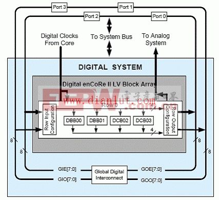
图2.CY7C603xx数字系统方框图
The Analog System
The analog system consists of two configurable blocks. Analog peripherals are very flexible and may be customized to support specific application requirements. Some of the common analog functions for this device (available as user modules) are:
■ Analog-to-digital converters (single with 8-bit resolution)
■ Pin-to-pin comparators
■ Single-ended comparators with absolute (1.3V) reference
■ 1.3V reference (as a System Resource)
Analog blocks are provided in columns of two, which includes one CT (Continuous Time - ACE00 or ACE01) and one SC (Switched Capacitor - ASE10 or ASE11) blocks.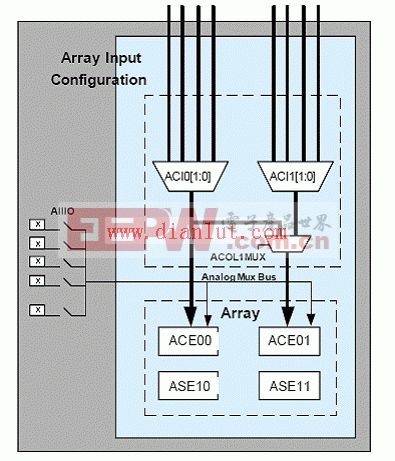
图3.CY7C603xx模拟系统方框图

评论