ADC and DAC Glossary


ADC and DAC Glossary
Abstract: This document collects and defines technical terms commonly used with analog-to-digital converters (ADCs) and digital-to-analog converters (DACs).
Acquisition Time
Acquisition time is the interval between the release of the hold state (imposed by the input circuitry of a track-and-hold) and the instant at which the voltage on the sampling capacitor settles to within 1 LSB of a new input value. The equation for acquisition time (Tacq) is: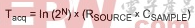 where RSOURCE is the source impedance, CSAMPLE is the sampling capacitance, and N is the number of resolution bits.
Aliasing
In sampling theory, input-signal frequencies that exceed the Nyquist frequency are "aliased." That is, they are "folded back" or replicated at other positions in the spectrum above and below the Nyquist frequency. To prevent aliasing, you must adequately filter all undesired signals so the ADC does not digitize them. Aliasing can be used to advantage when undersampling.See also application note Filter Basics: Anti-Aliasing
Aperture Delay
Aperture delay (tAD) in an ADC is the interval between the sampling edge of the clock signal (the rising edge of the clock signal in the figure) and the instant when the sample is taken. The sample is taken when the ADC's track-and-hold goes into the hold state. 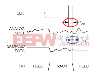
Binary Coding (Unipolar)
Straight binary is a coding scheme typically used for unipolar signals. The binary code (zero scale to full scale) ranges from all zeros (00...000) to the positive full-scale value of all ones (11...111). Midscale is represented by a one (the MSB) followed by all zeros (10...000). This code is similar to offset binary coding, which accommodates the positive and negative values of bipolar transfer functions.
Bipolar Inputs
The term 'bipolar' indicates that the signal swings above and below some reference level. In single-ended systems, the input is typically referenced to analog ground, so a bipolar signal is one that swings above and below ground. In differential systems, where the signal is not referenced to ground but where the positive input is referenced to the negative input, a bipolar signal is one in which the positive input swings above and below the negative input.
Common-Mode Rejection (CMR)
Common-mode rejection is the ability of a device to reject a signal that is common to both inputs. The common-mode signal can be an AC or DC signal, or a combination of the two. Common-mode rejection ratio (CMRR) is the ratio of the differential signal gain to the common-mode signal gain. CMRR is often expressed in decibels (dB).
Crosstalk
Crosstalk is a measure of how well each analog input is isolated from the others. For an ADC with more than one input channel, crosstalk is the amount of signal that couples from one analog input into another. This value is typically specified in decibels (dB). For a DAC with more than one input channel, crosstalk is the amount of noise that appears on a DAC output when another DAC output channel is updated.
Differential Nonlinearity (DNL) Error
For an ADC, the analog-input levels that trigger any two successive output codes should differ by one LSB (DNL = 0). Any deviation from one LSB is defined as DNL. For a DAC, DNL error is the difference between the ideal and the measured output responses for successive DAC codes. An ideal DAC response would have analog output values exactly one code (LSB) apart (DNL = 0). (A DNL specification of greater than or equal to 1LSB guarantees monotonicity.) (See "Monotonic.")
Effective Number Of Bits (ENOB)
ENOB specifies the dynamic performance of an ADC at a specific input frequency and sampling rate. An ideal ADC's error consists only of quantization noise. As the input frequency increases, the overall noise (particularly in the distortion components) also increases, thereby reducing the ENOB and SINAD. (See 'Signal-to-Noise and Distortion Ratio (SINAD).') ENOB for a full-scale, sinusoidal input waveform is computed from:
Force-Sense Outputs
This is a measurement technique in which a voltage (or current) is forced at a remote point in a circuit, and the resulting current (or voltage) is measured (sensed). DACs with integrated output amplifiers, for example, sometimes include force-sense outputs. The inverting input of the output amplifier is available for external connection, and the feedback path must be closed externally.
Full-Power Bandwidth (FPBW)
An ADC is operated with an applied analog input at or near the converter's specified full-scale amplitude. The input frequency is increased to the point at which the amplitude of the digitized conversion result has decreased by 3dB. That input frequency is defined as the full-power input bandwidth.
Full-Scale (FS) error
Full-scale error is the difference between the actual value that triggers the transition to full-scale and the ideal analog full-scale transition value. Full-scale error equals offset error + gain error, as shown in this figure.
Gain Error
The gain error of an ADC or DAC indicates how well the slope of an actual transfer function matches the slope of the ideal transfer function. Gain error is usually expressed in LSB or as a percent of full-scale range (%FSR), and it can be calibrated out with hardware or in software. Gain error is the full-scale error minus the offset error.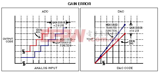
Gain Matching
Gain matching indicates how well the gains of all channels in a multichannel ADC are matched to each other. To calculate gain matching, apply the same input signal to all channels, and report the maximum deviation in gain, typically in dB.
Glitch Impulse
Glitch impulse is the voltage transient that appears at the DAC output when a major-carry transition occurs. Typically measured as nVs, it equals the area under the curve on a voltage-vs-time graph.
Harmonic
A harmonic of a periodic signal is a sinewave multiple of the signal's fundamental frequency.
Integral Nonlinearity (INL) Error
For data converters, INL is the deviation of an actual transfer function from a straight line. After nullifying offset and gain errors, the straight line is either a best-fit straight line or a line drawn between the end points of the transfer function. INL is often called 'relative accuracy.'See also application note INL/DNL Measurements for High-Speed Analog-to-Digital Converters (ADCs).
Major-Carry Transition
At the major-carry transition (around mid-scale), either the MSB changes from low to high and all other bits change from high to low, or the MSB changes from high to low and all other bits change from low to high. For example, 01111111 to 10000000 is a major-carry transition. Major-carry transitions often produce the worst switching noise. (See Glitch Impulse.)
Monotonic
A sequence increases monotonically if for every n, Pn + 1 is greater than or equal to Pn. Similarly, a sequence decreases monotonically if for every n, Pn + 1 is less than or equal to Pn. A DAC is monotonic if the analog output always increases as the DAC-code input increases. An ADC is monotonic if the digital output code always increases as the ADC analog input increases. A converter is guaranteed monotonic if the DNL error is no greater than ±1LSB
Most Significant Bit (MSB)
In a binary number, the MSB is the most weighted bit in the number. Typically, the MSB is the left-most bit.
Multiplying DAC (MDAC)
A multiplying DAC allows an AC signal to be applied to the reference input. By feeding the signal of interest into the reference input and by using the DAC codes to scale the signal, the DAC can be used as a digital attenuator.
No Missing Codes
An ADC has no missing codes if it produces all possible digital codes in response to a ramp signal applied to the analog input.
Nyquist Frequency
The Nyquist principle states that, to allow an analog signal to be completely represented with no aliasing effects, the ADC's sampling rate must be at least twice the maximum bandwidth of the signal. This maximum bandwidth is called the Nyquist frequency.
Offset Binary Coding
Offset binary is a coding scheme often used for bipolar signals. In offset binary coding, the most negative value (negative full scale) is represented by all zeros (00...000) and the most positive value (positive full scale) is represented by all ones (11...111). Zero-scale is represented by a one (MSB) followed by all zeros (10...000). This scheme is similar to straight binary coding, which is typically used for unipolar signals. (See Binary Coding, Unipolar.)
Offset Error (Bipolar)
The measurement of offset error in bipolar converters is similar to that of offset error in unipolar converters. However, the error measured at zero-scale is at the midpoint of the bipolar transfer functions. (See Offset Error (Unipolar).)
Offset Error (Unipolar)
Offset error, often called 'zero-scale' error, indicates how well the actual transfer function matches the ideal transfer function at a single point. For an ideal data converter, the first transition occurs at 0.5LSB above zero. For an ADC, the zero-scale voltage is applied to the analog input and is increased until the first transition occurs. For a DAC, offset error is the analog output response to an input code of all zeros.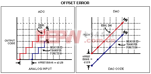
Oversampling
For an ADC, sampling the analog input at a rate much higher than the Nyquist frequency is called oversampling. Oversampling improves the ADC's dynamic performance by effectively reducing its noise floor. Improved dynamic performance leads, in turn, to higher resolution. Oversampling is the basis of sigma-delta ADCs.See also application note Demystifying Sigma-Delta ADCs
Phase-Matching
Phase matching indicates how well matched are the phases of identical signals applied to all channels in a multichannel ADC. Phase matching is the maximum deviation in phase among all the channels, and is typically reported in degrees.
Power-Supply Rejection (PSR)
Power Supply Rejection Ratio (PSRR) is the ratio of the change in DC power supply voltage to the resulting change in full-scale error, expressed in dB.
Quantization Error
For an ADC, quantization error is defined as the difference between the actual analog input and the digital representation of that value. (See 'Quantization.')
Ratiometric Measurement
Instead of a constant-valued reference voltage, a fraction of the signal applied to the transducer (i.e., the load cell or bridge) is applied to the ADC's voltage reference input. This type of measurement, called ratiometric, eliminates any errors introduced by changes in the reference voltage. An example of ratiometric measurement using a resistive bridge is shown in the figure below.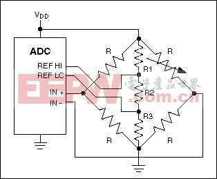
Root Mean Square (RMS)
2/2 (or 0.707) times the peak value, which is 0.354 times the peak-to-peak value.
Sampling Rate/Frequency
Sampling rate or sampling frequency, specified in samples per second (sps), is the rate at which an ADC acquires (samples) the analog input. For ADCs that perform one sample per conversion (such as SAR, flash, and pipeline ADCs), the sampling rate is also referred to as the throughput rate. For sigma-delta ADCs, the sampling rate is typically much higher than the output data rate.
Settling Time
For a DAC, settling time is the interval between a command to update (change) its output value and the instant it reaches its final value, within a specified percentage. Settling time is affected by the slew rate of an output amplifier and by the amount of amplifier ringing and signal overshoot. For an ADC, it is essential that the time required for voltage on the sampling capacitor to settle to within 1 LSB be less than the converter's acquisition time.
Signal-to-Noise And Distortion (SINAD)
SINAD is the ratio of the RMS value of the sinewave (input for an ADC, or reconstructed output for a DAC) to the RMS value of the converter noise plus distortion (without the sinewave). RMS noise plus distortion includes all spectral components up to the Nyquist frequency, excluding the fundamental and the DC offset. SINAD is typically expressed in dB.
Signal-to-Noise Ratio (SNR)
SNR is the ratio of the amplitude of the desired signal to the amplitude of the noise signals at a given point in time. For a waveform perfectly reconstructed from digital samples, the theoretical maximum SNR is the ratio of the full-scale analog input (RMS value) to the RMS quantization error (residual error).The ideal, theoretical minimum ADC noise is caused by quantization error only and results directly from the ADC's resolution (N bits): (Actual ADCs produce thermal noise, reference noise, clock jitter, etc., in addition to quantization noise.)
Signed Binary Coding
Signed binary is a coding scheme in which the MSB represents the sign (positive or negative) of a binary number. Thus, the 8-bit representation of -2 is 10000010, and the representation of +2 is 00000010.Slew Rate
Small-Signal Bandwidth (SSBW)
To measure SSBW, apply to an ADC an analog input signal of sufficiently small amplitude that its slew rate does not limit the ADC performance. Then, sweep the input frequency up to the point where the amplitude of the digitized conversion result decreases by -3dB. SSBW is often limited by the performance of the associated track-and-hold amplifier.
Spurious-Free Dynamic Range (SFDR)
SFDR is the ratio of the RMS amplitude of the fundamental (maximum signal component) to the RMS value of the next largest spurious component, excluding DC offset. SFDR is specified in decibels relative to the carrier (dBc).
Total Harmonic Distortion (THD)
THD measures the distortion content of a signal, and is specified in decibels relative to the carrier (dBc). For ADCs, THD is the ratio of the RMS sum of the selected harmonics of the input signal to the fundamental itself. Only harmonics within the Nyquist limit are included in the measurement.
Track-and-Hold
Track-and-hold, often called 'sample-and-hold,' refers to the input-sampling circuitry of an ADC. The most basic representation of a track-and-hold input is an analog switch and a capacitor. (See figure.) The circuit is in 'track' mode when the switch is closed. When the switch opens, the last instantaneous value of the input is held on the sampling capacitor, and the circuit is in 'hold' mode.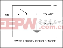
Two's Complement Coding
Two's complement is a digital coding scheme for positive and negative numbers that simplifies addition and subtraction computations. In this scheme, the 8-bit representation of -2 is 11111110, and the representation of +2 is 00000010.
Undersampling
Undersampling is a technique in which the ADC sampling rate is lower than the analog input frequency?a condition that causes aliasing. Given the Nyquist criterion, it is natural to expect that undersampling would result in a loss of signal information. However, with proper filtering of the input signal and with proper selection of the analog input and sampling frequencies, the aliased components that contain the signal information can be shifted from a higher frequency to a lower frequency and then converted. This method effectively uses the ADC as a downconverter, shifting higher-bandwidth signals into the ADC's desired band of interest. For this technique to be successful, the bandwidth of the ADC's track-and-hold must be capable of handling the highest frequency signals anticipated.
Unipolar
For an ADC with single-ended analog input, the unipolar input ranges from zero-scale (typically ground) to full scale (typically the reference voltage). For an ADC with differential inputs, the unipolar input ranges from zero-scale to full-scale, with the input measured as the positive input with respect to the negative input.
Zero-Scale Error
See offset error (unipolar)
评论