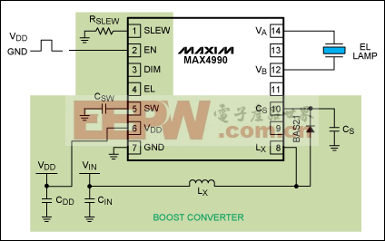
Abstract: The AC waveform (for voltage level and frequency) across an electroluminescent (EL) lamp affects brightness, current consumption, and the color of emitted light, and adjustment of the output waveform's slew rate affects the audible noise generated by the lamp itself. Consequently, the MAX4990 circuit must be optimized according to the requirements for each application. This application note provides information regarding circuit optimization and indicates the best external components to be used with the MAX4990. IntroductionThe MAX4990 is a high-voltage DC-AC converter designed to drive electroluminescent (EL) lamps. To generate the high voltage necessary to drive an EL panel, the MAX4990 utilizes a high-frequency boost converter and a high-voltage, full-bridge output stage to generate a high-voltage AC waveform suitable for driving the EL lamp. The MAX4990's proprietary acoustic noise-reduction circuit controls the slew rate of the AC voltage driving the EL panel, thus reducing audible noise.The MAX4990 provides a DIM pin that allows the user to set the EL output voltage through a PWM or DC analog voltage, or by connecting a resistor to GND. A capacitor placed in parallel to the resistor on the DIM pin allows the user to program a slow turn-on/off time for the MAX4990.An EL lamp's brightness, current consumption, and color of emitted light are affected by the AC waveform (for voltage level and frequency) across the lamp. Adjustment of the output waveform's slew rate affects the audible noise generated by the lamp itself. Therefore, depending on requirements for each application, the MAX4990 circuit must be optimized. This application note discusses circuit optimization and selection of the external components that should be used with MAX4990.EL Lamps and Their PropertiesEL lamps are constructed of light-emitting layers of phosphor particles evenly dispersed on dielectric material. These layers are sandwiched between rear and transparent front electrodes, which are then covered by protective polymer layer.Generally, EL lamps behave as capacitors, as shown in Figure 1. A change in frequency has an affect on the color of the emitted light, but both applied voltage and frequency affect EL lamp brightness. Raising voltage and/or frequency increases lamp brightness, but it also affects lamp life. In general, increasing lamp frequency (fEL) decreases lamp life more rapidly than increasing voltage. EL lamp life is most commonly specified in terms of time to half luminance (TTHL), or 'half-life,' which is the time it takes for the brightness of the EL lamp to decrease to half of its initial brightness at a given voltage and frequency. TTHL specifications are generally provided by the EL lamp manufacturer and specified in terms of thousands of hours. TTHL is not usually a concern for handheld products in which the lamp does not remain on for very long periods of time.In general, there are two types of EL lamps available: high-voltage EL lamps and low-voltage EL lamps. High-voltage EL lamps have a much higher threshold voltage than low-voltage EL lamps, meaning that a higher peak-to-peak voltage is required across a high-voltage EL lamp for it to start illuminating. High-voltage EL lamps are targeted to be driven with transformer-based drivers, whereas low-voltage EL lamps are meant to be driven by IC-based EL drivers. Hence, selection of the appropriate EL lamp for each application becomes the first step towards optimizing a circuit. A change in frequency has an affect on the color of the emitted light, but both applied voltage and frequency affect EL lamp brightness. Raising voltage and/or frequency increases lamp brightness, but it also affects lamp life. In general, increasing lamp frequency (fEL) decreases lamp life more rapidly than increasing voltage. EL lamp life is most commonly specified in terms of time to half luminance (TTHL), or 'half-life,' which is the time it takes for the brightness of the EL lamp to decrease to half of its initial brightness at a given voltage and frequency. TTHL specifications are generally provided by the EL lamp manufacturer and specified in terms of thousands of hours. TTHL is not usually a concern for handheld products in which the lamp does not remain on for very long periods of time.In general, there are two types of EL lamps available: high-voltage EL lamps and low-voltage EL lamps. High-voltage EL lamps have a much higher threshold voltage than low-voltage EL lamps, meaning that a higher peak-to-peak voltage is required across a high-voltage EL lamp for it to start illuminating. High-voltage EL lamps are targeted to be driven with transformer-based drivers, whereas low-voltage EL lamps are meant to be driven by IC-based EL drivers. Hence, selection of the appropriate EL lamp for each application becomes the first step towards optimizing a circuit. MAX4990 Circuit OptimizationCircuit optimization consists of selecting the external components such that the required parameters for each EL panel application are met. These parameters consist of: output voltage, current draw, lamp frequency, lamp brightness requirement, lamp-generated audible noise, and output waveform shape.DC-DC ConversionHigh DC-output-voltage generation is accomplished by a boost converter. The boost converter (Figure 2) consists of: an internal DMOS switch (Q), internal switch oscillator, external inductor (LX), external fast reverse-recovery diode (D), and external high-voltage capacitor (CS).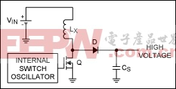 The switching frequency (fSW) of LX can be set by either of the following: The switching frequency (fSW) of LX can be set by either of the following: - A combination of RSLEW resistor and CSW capacitor values from the SLEW and SW pins (respectively) to GND, as indicated in Figure 3.
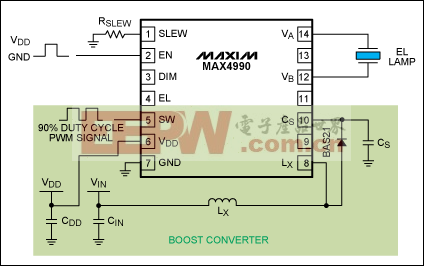
  - Driving a PWM signal directly into the SW pin, as illustrated in Figure 4.
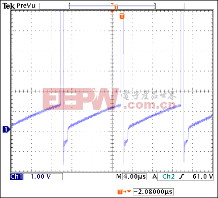
 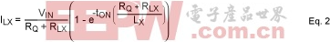 Where:To determine whether the inductor is being saturated, the waveform on the node between LX and D (Figure 5) must be monitored if there are no current probes available. Where:To determine whether the inductor is being saturated, the waveform on the node between LX and D (Figure 5) must be monitored if there are no current probes available.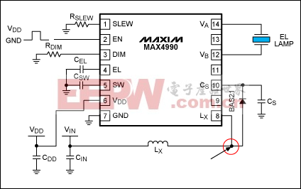 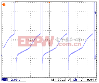 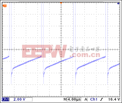 We also need to make sure that LX has enough time to discharge its stored energy to CS through the external diode so as to prevent inductor saturation. This is done by selecting the appropriate fSW for LX.The diode's reverse-recovery time becomes important, as the diode must contain all the energy transferred from LX in CS. Therefore, a diode with a fast reverse-recovery time, such as the BAS21 or BAS20, is recommended for use with the MAX4990.The CS value needs to be selected based on the lamp size and the amount of ripple that can be tolerated on the output waveform. Typically, a CS value of about 1/10 of the EL lamp capacitance is recommended. For any given fSW, larger CS values reduce the ripple on the output waveform. In general, higher inductor switching frequencies are recommended when smaller CS values are selected. We also need to make sure that LX has enough time to discharge its stored energy to CS through the external diode so as to prevent inductor saturation. This is done by selecting the appropriate fSW for LX.The diode's reverse-recovery time becomes important, as the diode must contain all the energy transferred from LX in CS. Therefore, a diode with a fast reverse-recovery time, such as the BAS21 or BAS20, is recommended for use with the MAX4990.The CS value needs to be selected based on the lamp size and the amount of ripple that can be tolerated on the output waveform. Typically, a CS value of about 1/10 of the EL lamp capacitance is recommended. For any given fSW, larger CS values reduce the ripple on the output waveform. In general, higher inductor switching frequencies are recommended when smaller CS values are selected.Output Waveform Across the EL LampThe MAX4990 uses a high-voltage, full-bridge output stage to convert the high voltage generated by the boost converter to an AC waveform suitable for driving the EL panel. Output voltage, the output waveform's slew rate, slow turn-on and turn-off, and the output waveform's frequency are adjustable to provide the highest degree of freedom when optimizing the circuit so that the best results can be obtained for each application.Optimization of the EL driver circuit is dependent upon many different variables. The best way to optimize a circuit is to prioritize the variables for each application. For example, because EL lamps are used for backlighting purposes, lamp brightness can often be a fixed value, thereby reducing the set of variables and simplifying the optimization process.An EL lamp's brightness and color of emitted light are dependent upon the output voltage frequency. Depending on the lamp color, different frequency ranges must be used.The first step toward optimizing the output waveform is to select the appropriate fEL based on the desired lamp color.Lamp frequency is adjusted by either: - A combination of the RSLEW and CEL capacitor values from the SLEW and EL pins (respectively) to GND. The fEL can be calculated as follows:
 - Applying a clock signal to the EL pin. In this case, the fEL is ¼th of the clock frequency.
Lamp brightness intensifies as frequency is increased, as illustrated in Figure 8. Keep in mind that, as the fEL is increased, a higher amount of current from a given input voltage is required to drive a given lamp size.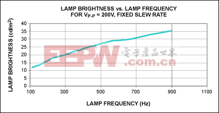  - A PWM signal applied to the DIM pin. The PWM signal's duty cycle is internally translated from 0 to 1.22V.
- A DC voltage applied to the DIM pin. Increasing the DC voltage from 0.35V to 1.3V increases the VP-P across the lamp from 70V to 250V.
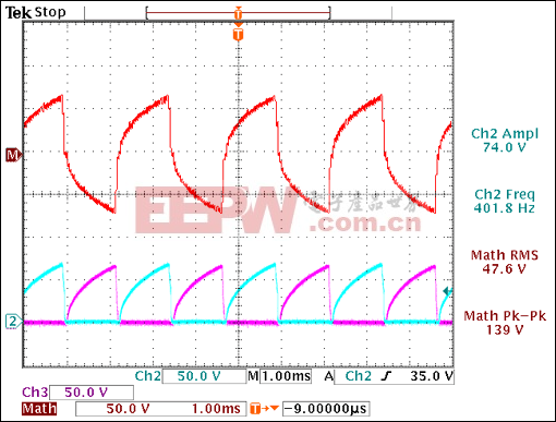
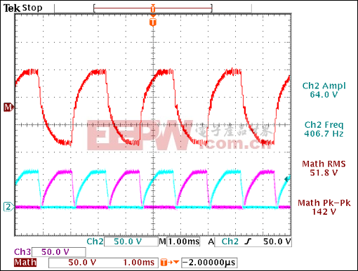
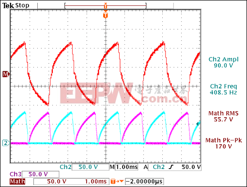
EL lamp brightness increases as the output voltage across the lamp is increased (see Figure 9). Applying a higher voltage across the lamp requires that a higher current is drawn from the inductor's input voltage source.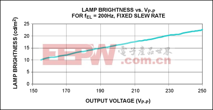 The output waveform's slew rate is controlled through RSLEW, which is connected from the SLEW pin to GND. This slew rate can be calculated as follows: The output waveform's slew rate is controlled through RSLEW, which is connected from the SLEW pin to GND. This slew rate can be calculated as follows: An ideal output slew rate that minimizes audible noise generated by the lamp is dependent upon the lamp size and mechanical enclosure. Therefore, resonant frequency of the enclosure must be taken into account when selecting fEL for a given lamp size.A sinusoidal waveform is believed to be optimal for providing the least amount of audible noise generated by the lamp. However, a sinusoidal waveform also generates less brightness than a square waveform at a given voltage level and frequency. Hence, each circuit must be optimized according to the requirements for its individual application.As the slew rate of the output waveform is decreased, audible noise generated by the EL lamp is decreased and a lower amount of current is drawn. However, a slower slew rate does decrease lamp brightness, as seen in Figure 10. An ideal output slew rate that minimizes audible noise generated by the lamp is dependent upon the lamp size and mechanical enclosure. Therefore, resonant frequency of the enclosure must be taken into account when selecting fEL for a given lamp size.A sinusoidal waveform is believed to be optimal for providing the least amount of audible noise generated by the lamp. However, a sinusoidal waveform also generates less brightness than a square waveform at a given voltage level and frequency. Hence, each circuit must be optimized according to the requirements for its individual application.As the slew rate of the output waveform is decreased, audible noise generated by the EL lamp is decreased and a lower amount of current is drawn. However, a slower slew rate does decrease lamp brightness, as seen in Figure 10.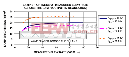 For applications sensitive to audible noise, it is not recommended to allow the output waveform to enter regulation (i.e., the output waveform should not have a plateau at the top of it). After selecting the slew rate for the application, the output voltage must be adjusted to get the best waveform shape across the lamp.When using MAX4990, the optimum waveform for applications sensitive to audible noise is thought to be the waveform shape shown in Figure 11. For applications sensitive to audible noise, it is not recommended to allow the output waveform to enter regulation (i.e., the output waveform should not have a plateau at the top of it). After selecting the slew rate for the application, the output voltage must be adjusted to get the best waveform shape across the lamp.When using MAX4990, the optimum waveform for applications sensitive to audible noise is thought to be the waveform shape shown in Figure 11.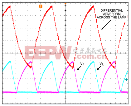 This slow turn-on/turn-off feature is controlled by connecting a capacitor, CDIM, in parallel with RDIM to GND (Figure 12). This slow turn-on/turn-off feature is controlled by connecting a capacitor, CDIM, in parallel with RDIM to GND (Figure 12).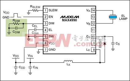   Figure 13 shows the affect of using CDIM in parallel with RDIM for slow turn-on/turn-off of the EL lamp. Figure 13 shows the affect of using CDIM in parallel with RDIM for slow turn-on/turn-off of the EL lamp.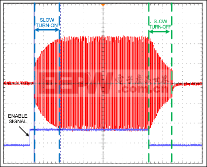 The on-board 555 timer enables the user to choose different inductor switching frequencies, as well as fEL, without changing the CSW and CEL values and without the RSLEW value having any affect on these frequencies.It is recommended that the following equipment is used for optimizing the MAX4990 circuit: The on-board 555 timer enables the user to choose different inductor switching frequencies, as well as fEL, without changing the CSW and CEL values and without the RSLEW value having any affect on these frequencies.It is recommended that the following equipment is used for optimizing the MAX4990 circuit: - Power supply
- Multimeter in series with the power supply to measure the current draw
- 2-channel oscilloscope to monitor the waveform and its shape across the lamp (connect one channel to VA and another to VB; if desired, view the differential voltage across the lamp by adding VA to the inverted signal from VB)
- Brightness measurement meter or specifications from the lamp manufacturer regarding the voltage and frequency required to obtain certain brightness
The following procedure details how to use the MAX4990 EV kit to optimize a circuit when driving a 20nF green lamp to provide 37cd/m² with fEL = 400Hz when VDD = VBATT = 3.6V. Note that the inductor used on the EV kit is a 220µH inductor from TOKO (D312C series, part number 1001BS-221M), and its CS value is 3.3nF (150V).To optimize the circuit using the 555 timer on the MAX4990 EV kit, the following steps must be taken when placing the jumper on JU4 and JU5: - Set VR1 to 0Ω with JU1 in positions 2 and 3. Put the JU4 and JU5 jumpers in place.
- Using a 3.6V supply, power the EV kit with an EL lamp connected to it and JU8 in place.
- Use VR3 to set the fEL to 400Hz.
- Use VC1 to set the current draw to its minimum.
- Use VR2, with JU3 in positions 1 and 2, to set the output voltage at a level that indicates the circuit is not in regulation. This means that the output waveform does not have a plateau at the top of it, as seen in Figure 14.
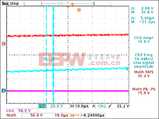
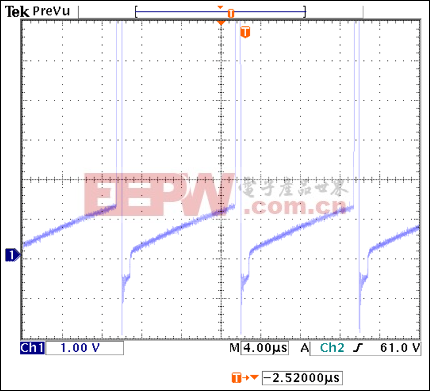
 - Measure fSW. This can be done by expanding the timescale of either VA or VB to the point that you can see the small steps on the output waveform, as in Figure 15.
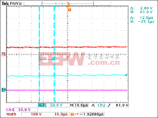
  - Change fSW through VC1 to increase the output voltage to a level that approximately provides the desired brightness (Figure 16).
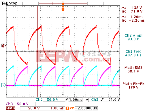
 - Check the waveform to make sure that the inductor is not saturated, as shown in Figure 17.
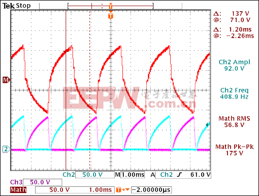
   IDD = 53mA, brightness = 38.5cd/m², RSLEW = 100kΩ, RDIM = 87kΩ IDD = 53mA, brightness = 38.5cd/m², RSLEW = 100kΩ, RDIM = 87kΩ - With JU1 in positions 2 and 3, use VR1 to change the slew rate of output waveform's rising and falling edges. Note that the faster slew rate (dV/dt) provides higher brightness, but it also causes the EL lamp to generate a higher audible noise (Figure 20).
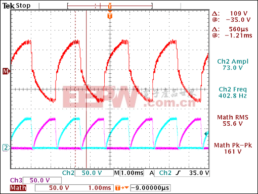
 - Repeat step 5 to make certain the device is not in regulation (Figure 21).
 - Repeat step 8 to check for inductor saturation (Figure 22).
  - Repeat step 5 to make certain the device is not in regulation (Figure 24).
 - Repeat steps 7, 8, 9, 11 and 5 (in this order) until you achieve the desired brightness with the appropriate waveform shape for your application (Figures 25 and 26).
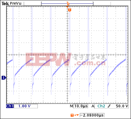 Figure 26. Repeating step 5 shows that the device is not in regulation.The following was measured for VDD = 3.6V: Figure 26. Repeating step 5 shows that the device is not in regulation.The following was measured for VDD = 3.6V: - Calculate fSW using equation 8 from step 6 (Figure 27).
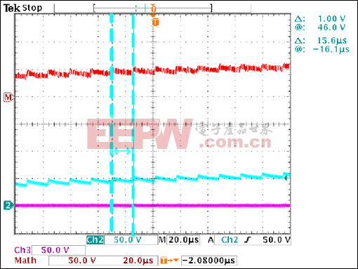  - Measure the RDIM and RSLEW values.RDIM = 239.4kΩ
- Note that the RSLEW value would be the value on VR1 + 100kΩ, as there is a 100kΩ resistor used on the EV kit in series with VR1. Make sure that power is disconnected from the EV kit when measuring the VR1 and VR2 values.
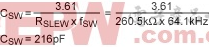
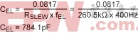
- Having measured fSW, fEL (400Hz), and both the RSLEW and RDIM values, calculate the CSW and CEL values to be used in your circuit using equations 1 and 3:
  - Select the closest available capacitor values to the values calculated for your circuit. Some minor adjustments to RSLEW and RDIM may be required based on the selected CSW and CEL values.
- Select CDIM based on the set RDIM value to achieve the desired slow turn-on/turn-off time.If the user replaces the inductor on the EV kit with an off-the-shelf inductor, the circuit will need to be re-optimized based around the new inductor. Additionally, changes in lamp size and available input voltage will require circuit optimization as well.When using the 555 timer, if fSW needs to be altered in order to optimize the circuit, the user must make sure that fSW has a duty cycle (DC) range of 88% to 90%. The DC range is set based on the following equation:

|


评论