ad637应用电路


ad637应用电路
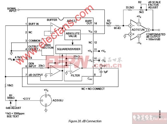
dB CALIBRATION
Refer to Figure 20:
Set V
= 1.00 V dc or 1.00 V rms IN
Adjust R1 for 0 dB out = 0.00 V
Set V = 0.1 V dc or 0.10 V rms IN
Adjust R2 for dB out = 2.00 VAny other dB reference can be used by setting VIN and R1 accordingly.
As with previous monolithic rms converters from Analog Devices, Inc., the AD637 has an auxiliary dB output available to users. The logarithm of the rms output signal is brought out to a separate pin, allowing direct dB measurement with a useful range of 60 dB. An externally programmed reference current allows the user to select the 0 dB reference voltage to correspond to any level between 0.1 V and 2.0 V rms.
评论