
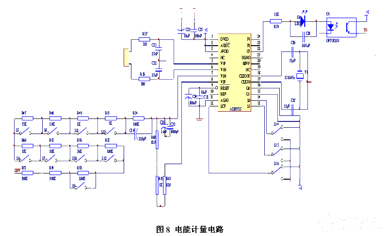
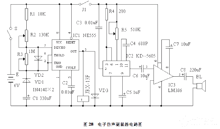
TDA7250引脚图及功能介绍,TDA7250内部方框原理图

TDA7250引脚图及功能介绍
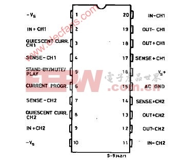
PIN FUNCTIONS
N° Name Function
1 VS – POWER SUPPLY Negative Supply Voltage.
2 NON–INV. INP. CH. 1 Channel 1 Input Signal.
3 QUIESC. CURRENT
CONTR. CAP. CH1
This capacitor works as an integrator, to control the quiescent current to output
devices in no-signal conditions on channel 1.
4 SENSE (–) CH. 1 Negative voltage sense input for overload protection and for automatic quiescent
current control.
5 ST. BY / MUTE / PLAY Three-functions Terminal.
For VIN = 1 to 3 V, the device is in MUTE and only quiescent current flows in
the power stages ; - for VIN 1 V, the device is in STAND-BY mode and no
quiescent current is present in the power stages ; - for VIN 3 V, the devic
6 CURRENT PROGRAM High Impedance Power-stages Monitor.
7 SENSE (–) CH. 2 Negative Voltage Sense Input for Overload Protection and for Automatic
Quiescent Current Control.
8 QUIESC. CURRENT
CONTR. CAP. CH. 2
This capacitor works as an integrator, to control the quiescent current to output
devices in no-signal conditions on channel 2. If the voltage at its terminals drops
under 250 mV, it also resets the device from high-impedance state of output
stages.
9 NON–INV. INP. CH. 2 Channel 2 Input Signals.
10 Vs – POWER SUPPLY Negative Supply Voltage.
11 INVERT. INP. CH. 2 Feedback from Output (channel 2).
12 OUT (–) CH. 2 Out Signal to Lower Driver Transistor of Channel 2.
13 OUT (+) CH. 2 Out Signal to Higher Driver Transistor of Channel 2.
14 SENSE (+) CH. 2 Positive Voltage Sense Input for Overload Protection and for Automatic
Quiescent Current Control.
15 COMMON AC GROUND AC Input Ground in MUTE Condition.
16 VS + POWER SUPPLY Positive Supply Voltage.
17 SENSE (+) CH. 1 Positive Voltage Sense Input for Overload Protection and for Automatic
Quiescent Current Control.
18 OUT (+) CH. 1 Out Signal to High Driver Transistor of Channel 1.
19 OUT (–) CH. 1 Out Signal to Low Driver Transistor of Channel 1.
20 INVERT. INP. CH. 1 Feedback from Output (channel 1).
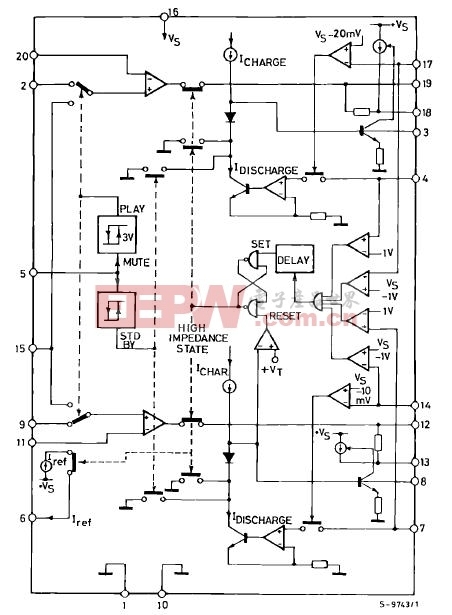
TDA7250内部方框原理图
评论