DS1306应用电路 (带有闹钟的串行实时时钟)
DS1306应用电路 (带有闹钟的串行实时时钟)
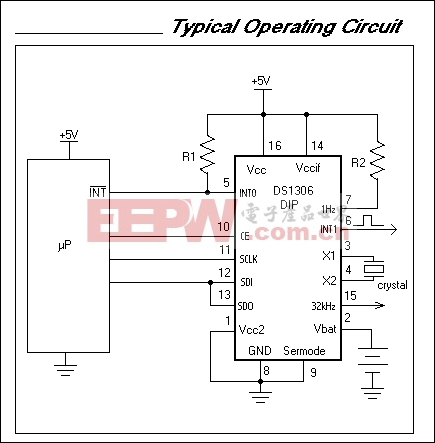 An interface logic-power supply input pin (VCCIF) allows the DS1306 to drive SDO and 32kHz pins to a level that is compatible with the interface logic. This allows an easy interface to 3V logic in mixed supply systems. The DS1306 offers dual-power supplies as well as a battery-input pin. The dual-power supplies support a programmable trickle charge circuit that allows a rechargeable energy source (such as a super cap or rechargeable battery) to be used for a backup supply. The VBAT pin allows the device to be backed up by a non-rechargeable battery. The DS1306 is fully operational from 2.0V to 5.5V.Two programmable time-of-day alarms are provided by the DS1306. Each alarm can generate an interrupt on a programmable combination of seconds, minutes, hours, and day. "Don't care" states can be inserted into one or more fields if it is desired for them to be ignored for the alarm condition. A 1Hz and a 32kHz clock output are also available.The DS1306 supports a direct interface to SPI serial data ports or standard 3-wire interface. An easy-to use address and data format is implemented in which data transfers can occur 1-byte at a time or in multiple-byte Burst Mode®.


评论