MAX19994/MAX19994A应用电路
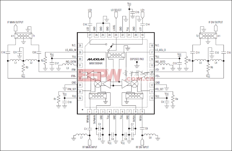
MAX19994/MAX19994A典型应用电路
应用/使用
cdma2000®基站In addition to offering excellent linearity and noise performance, the device also yields a high level of component integration. This device includes two double-balanced passive mixer cores, two LO buffers, a dual-input LO selectable switch, and a pair of differential IF output amplifiers. Integrated on-chip baluns allow for single-ended RF and LO inputs. The MAX19994A requires a nominal LO drive of 0dBm and a typical supply current of 330mA at VCC = 5.0V, or 264mA at VCC = 3.3V. The MAX19994A is pin compatible with the MAX9985/MAX9995/MAX19985A/MAX19993/MAX19995/MAX19995A series of 700MHz to 2500MHz mixers and pin similar with the MAX19997A/MAX19999 series of 1850MHz to 4000MHz mixers, making this entire family of downconverters ideal for applications where a common PCB layout is used across multiple frequency bands. The device is available in a 6mm x 6mm, 36-pin thin QFN package with an exposed pad. Electrical performance is guaranteed over the extended temperature range, from TC = -40°C to +85°C.


评论