
M4N25管脚说明及内部结构图 (含封装尺寸)

The M4N25 device consists of a gallium arsenide infrared emitting diode
optically coupled to a silicon NPN phototransistor detector.
Most Economical Optoisolator Choice for Medium Speed, Switching Applications
Meets or Exceeds All JEDEC Registered Specifications
M4N25管脚引脚定义说明:
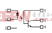
PIN 1. LED ANODE
2. LED CATHODE
3. N.C.
4. EMITTER
5. COLLECTOR
6. BASE
M4N25内部结构图


Applications
General Purpose Switching Circuits
Interfacing and coupling systems of different potentials and impedances
I/O Interfacing
Solid State Relays
MAXIMUM RATINGS (TA = 25°C unless otherwise noted)
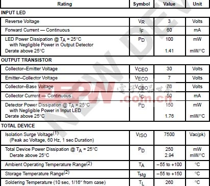
1. Isolation surge voltage is an internal device dielectric breakdown rating.
1. For this test, Pins 1 and 2 are common, and Pins 4, 5 and 6 are common.
2. Refer to Quality and Reliability Section in Opto Data Book for information on test conditions.
ELECTRICAL CHARACTERISTICS (TA = 25°C unless otherwise noted)(1)
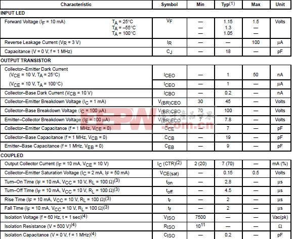
1. Always design to the specified minimum/maximum electrical limits (where applicable).
2. Current Transfer Ratio (CTR) = IC/IF x 100%.
3. For test circuit setup and waveforms, refer to Figure 14.
4. For this test, Pins 1 and 2 are common, and Pins 4, 5 and 6 are common.
M4N25封装尺寸
Package Dimensions in Inches (mm)


评论