
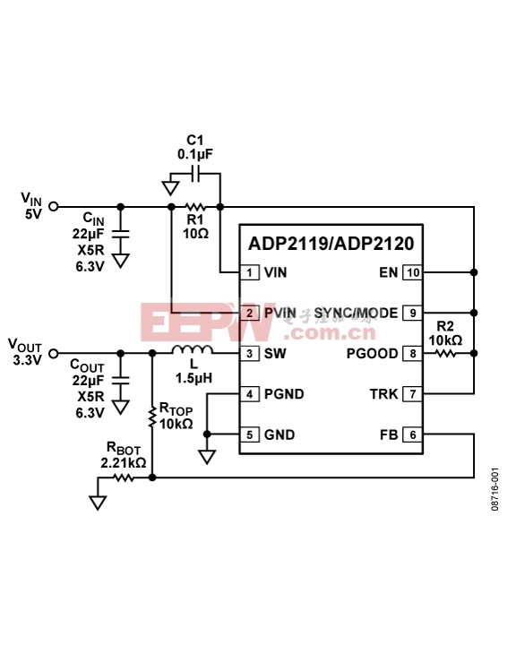
ADP2119/ADP2120应用电路 (5V输入3.3V输

The ADP2119/ADP2120 are low quiescent current, synchronous, step-down DC-to -DC regulators in a compact 3mm x 3mm LFCSP_WD package. Both Devices use current mode, constant frequency pulse-width modulation (PWM) control scheme for excellent stability and transient response. Under light load condition, they can be configured to operate in pulse frequency modulation (PFM) mode that reduces switching frequency to save power.
The ADP2119/ADP2120 can support input voltages from 2.3V to 5.5V. The output voltage can be adjusted from 0.6V to input voltage (VIN) for the adjustable version, while the fixed output version is available in preset output voltage options of 3.3V, 2.5V, 1.8V, 1.5V ,1.2V and 1.0V. The ADP2119/ADP2120 require minimal external parts and provide a high efficiency solution with their integrated power switches, synchronous rectifier, and internal compensation. Each IC draws less than 3 μA current from the input source when it is disabled. Other key features include under voltage lockout(UVLO), integrated soft start to limit inrush current at startup, overvoltage protection (OVP), over current protection (OCP) and thermal shutdown (TSD).

评论