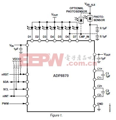
ADP8870典型应用电路及封装尺寸图


The ADP8870 combines a programmable backlight LED charge-pump driver with automatic phototransistor control of the brightness (LED current) and a PWM input to control the scale of the output current. This combination allows significant power savings because it automatically changes the current intensity based on the sensed ambient lighting levels and the display image content. It performs this function automatically, eliminating the need for a processor to monitor the photo-transistor. The light intensity thresholds are fully programmable via the I2C interface.
The ADP8870 allows up to six LEDs to be independently driven up to 30 mA (maximum). An additional seventh LED can be driven to 60 mA (maximum). All LEDs are individually programmable for minimum/maximum current and fade-in/fade-out times through an I2C interface. These LEDs can also be combined into groups to reduce the processor instructions during fade-in and fade-out.
Driving these components is a two-capacitor charge pump with gains of 1×, 1.5×, and 2×. This setup is capable of driving a maximum IOUT of 240 mA from a supply of 2.5 V to 5.5 V. A full suite of safety features, including short-circuit, overvoltage, and overtemperature protection, allows easy implementation of a safe and robust design. Additionally, input inrush currents are limited via an integrated soft start combined with controlled input-to-output isolation.
ADP8870典型应用电路
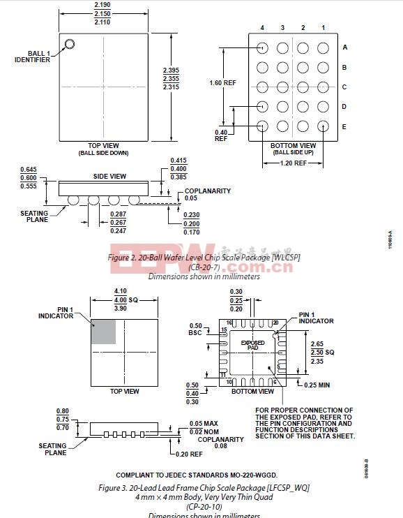
ADP8870封装尺寸图
评论