
74ls573中文资料

74LS573 八D 透明锁存
三态总线驱动输出
·置数全并行存取
·缓冲控制输入
·使能输入有改善抗扰度的滞后作用
原理:74LS573 的八个锁存器都是透明的D 型锁存器,当使能(G)为高时,Q 输出将随数据(D)输入而变。当使能为低时,输出将锁存在已建立的数据电平上。输出控制不影响锁存器的内部工作,即老数据可以保持,甚至当输出被关闭时,新的数据也可以置入。
这种电路可以驱动大电容或低阻抗负载,可以直接与系统总线接口并驱动总线,而不需要外接口。特别适用于缓冲寄存器,I/O 通道,双向总线驱动器和工作寄存器。
真值表:
输出enable
LatchENABLE启用
D输出
O
LHHHLHLLLLXQOHXXZH=高电平 L=低电平 ×=不定 Z=高阻态
QO=建立稳态输入条件前Q的电平
引脚功能表:
Pin Names管脚号
Description 功能
D0–D7 Data Inputs数据输入LE Latch Enable Input (Active HIGH) 锁存使能输入(高电平有效) OE 3-STATE Output Enable Input (Active LOW) 3态输出使能输入(低电平有效)O0–O7 3-STATE Latch Outputs 3态锁存输出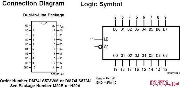
引脚图及功能图
Operating Conditions 操作条件
Symbol 符号Parameter 参数DM74LSUNIT 单位最小典型最大VCCSupply Voltage 电源电压4.7555.25VVIHHigh Level Input Voltage输入高电平电压2--VVILLOW Level Input Voltage 输入低电平电压--0.8VIOHHIGH Level Input Current输入高电平电流--2.6mAIOLLOW Level Output Current低电平输出电流--24mATAFree Air Operating Temperature工作温度0-70℃Note 1: The “Absolute Maximum Ratings” are those values beyond which the safety of the device cannot be guaranteed. The device should not be operated at these limits. The parametric values defined in the “Electrical Characteristics” table are not guaranteed at the absolute maximum ratings. The “Recommended Operating Conditions” table will define the conditions for actual device operation.Electrical Characteristics 直流电气特性Over recommended operating free air temperature range (unless otherwise noted)Symbol 符号Parameter 参数Conditions 条件最小典型最大UNIT 单位VIInput Clamp Voltage输入钳位电压VCC=最小, II=18 mA--1.5VVOHHigh Level OutputVoltage输出高电平电压VCC = 最小, IOH=最大,VIL = 最大2.73.4-VVOLLow Level OutputVoltage输出低电平电压 VCC = 最小, IOL=最大-0.350.5-VIH = 最小---VIOL=4 mA, VCC=最小----IIInput Current @ 最大Input Voltage输入电压VCC=最大, VI=7V--1mAIIHHIGH Level Input Current输入高电平电流VCC=最大, VI=2.7V--20μAIILLOW Level Input Current低电平输入电流VCC=最大, VI=0.4V--0.4mAIOSShort CircuitOutput Current输出短路电流VCC=最大(Note 3)30-130mA-ICCSupply Current电源电流VCC=最大--50mAIOZH3-STATE Outputoff Current High 3态输出高阻态时高电平电流VCC=VCCH VOZH=2.7V--20μAIOZL3-STATE Outputoff Current Low 3态输出高阻态时低电平电流VCC=VCCH VOZL=0.4V--20μANote 2: All typicals are at VCC = 5V, TA = 25℃.Note 3: Not more than one output should be shorted at a time, and the duration should not exceed one second.
Switching Characteristics at VCC = 5V and TA = 25℃ 交流开关特性Symbol 符号Parameter 参数RL=2kΩ, CL=50pFUNIT 单位最小最大tPLH tPHLPropagation Delay传播延迟 Data to Q-27 18nstPLH tPHLPropagation Delay传播延迟 LE to Q-36 25nstPZH tPZL3-STATE Enable Time3态启用时间 OE to Q-20 25nstPHZ tPLZ3-STATE Enable Time3态启用时间 OE to Q-20 25nsts(H)ts(L)Setup Time (High/Low) 设置时间(高/低)Data to LE3 7-nsth(H)th(L)Hold Time (High/Low)保持时间(高/低)Le Data to LE10 10-nstw(H) -Pulse Width (High) 脉冲宽度(高)LeData to LE15 --ns
评论