
CGD15FB45P参考设计电路|MOSFET驱动器应用电路

CGD15FB45P:6个输出通道;隔离式电源;短路保护;欠压保护
CGD15FB45P典型应用范围:用于1.2kV碳化硅MOSFET模块的6包驱动器;高达900VDC的直流总线电压CGD15FB45P参考设计应用电路:
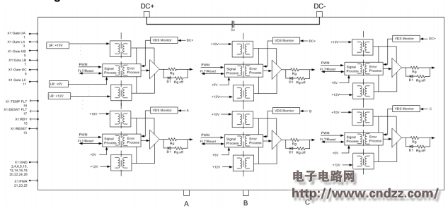
图1CGD15FB45P内部结构图
Default gate resistor for Rg is 10 for gate ON and OFF. The user can control the gate turn ON and OFF speed by changing Rg to a lower value and gain better MOSFET switching efficiency. The user can also control the Gate turn-ON and OFF speed independently by populating Rg.off and D1. Cs is made up of 3x 2.2nF, 1.2kV film Capacitors.
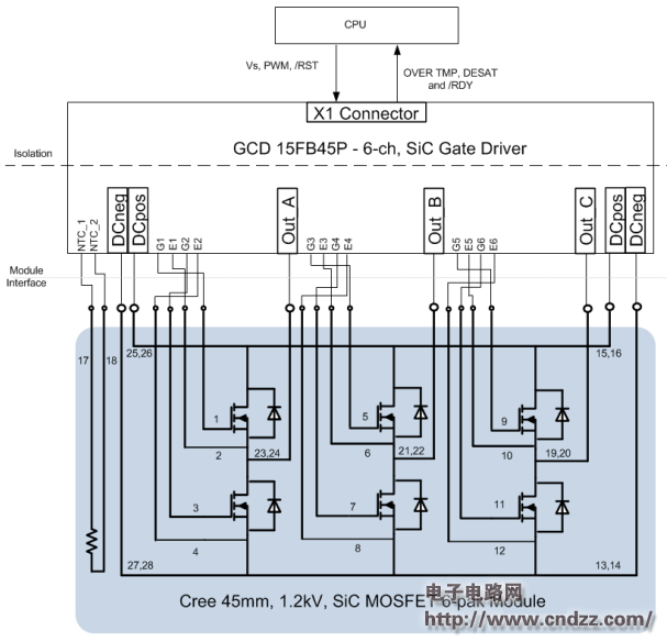
图2CGD15FB45P参考设计图
Attach the gate driver board to the power module via the 4x Module screw holes (see diagram below) using the recommended hardware in Table 1. Then solder the 28x solder pins via the solder pin holes to electrically connect the driver board to the power module. The solder must not exceed 260ºC and the solder per pin must not exceed 10 seconds. The solder joints should be in accordance with IPC A 610 Rev D (or later) – Class 3 to ensure an optimal connection between the module and gate driver board.
CGD15FB45P中文数据手册:点击下载
更多原理图及源代码热门应用电路:立刻点击
评论