
SSM2142参考设计电路|音频放大器应用电路

SSM2142特性:低失真;高压摆率15V/µs(典型值);输出短路保护;低成本
SSM2142典型应用范围:HiFi设备;电信系统;工业仪表
SSM2142参考设计应用电路:

图1SSM2142内部结构图
TheSSM2142 is an integrated differential-output buffer amplifier that converts a single-ended input signal to a balanced output signal pair with high output drive. By utilizing low noise thermally matched thin film resistors and high slew rate amplifiers, the SSM2142 helps maintain the sonic quality of audio systems by eliminating power line hum, RF interference,voltage drops, and other externally generated noise commonly encountered with long audio cable runs.
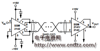
图2SSM2142参考设计图
TheSSM2142 is designed to provide excellent common-mode rejection, high output drive, and low signal distortion and noise in a balanced line-driving system. The differential output stage consists of twin cross-coupled unity gain buffer amplifiers with on-chip 50 ? series damping resistors.
SSM2142中文数据手册:点击下载
更多原理图及源代码热门应用电路:立刻点击
评论