
TPS82085参考设计电路|降压转换器应用电路

TPS82085特性:3A薄型MicroSiP电源模块;DCS-Control拓扑技术;效率高达95%;静态工作电流:17μA;工作温度范围:-40°C至125°C
TPS82085典型应用范围:电池供电类应用;固态硬盘;处理器电源;移动电话TPS82085参考设计应用电路:
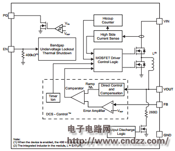
图1TPS82085内部结构图
The TPS82085 device is a 3-A step-down converter MicroSiP™ module optimized for small solution size and high efficiency. The power module integrates a synchronous step-down converter and an inductor to simplify design, reduce external components and save PCB area. The low profile and compact solution is suitable for automated assembly by standard surface mount equipment.
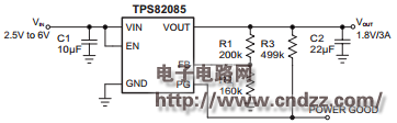
图2TPS82085参考设计图
To maximize efficiency, the converter operates in PWM mode with a nominal switching frequency of 2.4MHz and automatically enters Power Save Mode operation at light load currents. In Power Save Mode,the device operates with typically 17-μA quiescent current.
TPS82085中文数据手册:点击下载
更多原理图及源代码热门应用电路:立刻点击
评论