
ADS8684参考设计电路|模数转换器应用电路

ADS8684 是4通道集成数据采集系统,基于 16 位逐次逼近 (SAR) 模数转换器 (ADC),此篇主要介绍了ADS8684特性、应用范围、参考设计电路以及电路分析,帮助大家缩短设计时间。
ADS8684特性:
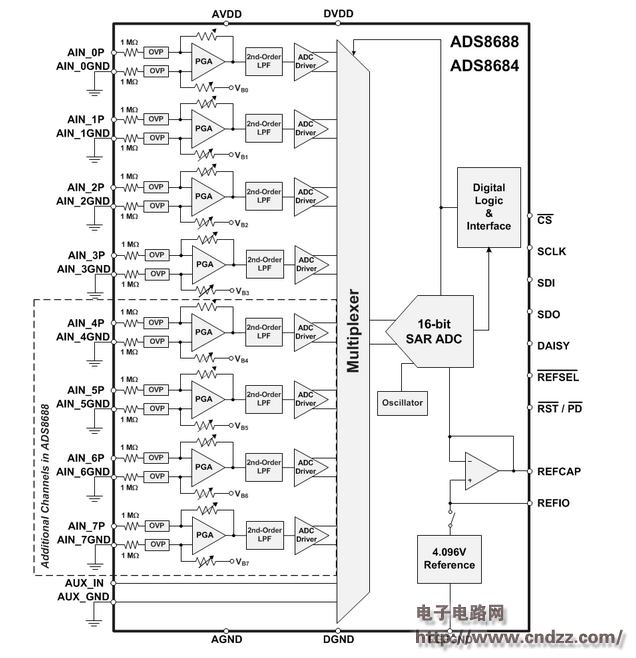
ADS8684提供了用于各输入通道的集成模拟前端电路(过压保护高达 ±20V)、支持自动和手动两种扫描模式的 4 通道多路复用器、以及低温度漂移的片上 4.096V 基准电压。 采用 5V 单模拟电源供电时,器件上的各输入通道均可支持双极输入以及单极输入。ADS8684还提供了用于连接数字主机的简单 SPI 兼容串行接口,并且支持以菊花链形式连接多个器件。
ADS8684典型应用范围包括:电力自动化、保护中继器、PLC 模拟输入模块
ADS8684内部结构框图:
ADS8684参考设计电路:
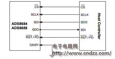
ADS8684应用电路分析:CS (Input): CS indicates an active-low, chip-select signal. CS is also used as a control signal to trigger a conversion on the falling edge. Each data frame begins with the falling edge of the CS signal. The analog input channel to be converted during a particular frame is selected in the previous frame. On the CS falling edge, the devices sample the input signal from the selected channel and a conversion is initiated using the internal clock. The device settings for the next data frame can be input during this conversion process. When the CS signal is high, the ADC is considered to be in an idle state. SCLK (Input): This pin indicates the external clock input for the data interface. All synchronous accesses to the device are timed with respect to the falling edges of the SCLK signal. SDI (Input): SDI is the serial data input line. SDI is used by the host processor to program the internal device registers for device configuration. At the beginning of each data frame, the CS signal goes low and the data on the SDI line are read by the device at every falling edge of the SCLK signal for the next 16 SCLK cycles. Any changes made to the device configuration in a particular data frame are applied to the device on the subsequent falling edge of the CS signal. SDO (Output): SDO is the serial data output line. SDO is used by the device to output conversion data. The size of the data output frame varies depending on the register setting for the SDO format; A low level on CS releases the SDO pin from the Hi-Z state. SDO is kept low for the first 15 SCLK falling edges. The MSB of the output data stream is clocked out on SDO on the 16th SCLK falling edge, followed by the subsequent data bits on every falling edge thereafter. The SDO line goes low after the entire data frame is output and goes to a Hi-Z state when CS goes high.
ADS8684中文资料:点击下载
带有原理图和源码的热门应用电路请见:www.cirmall.com
评论