
SSL5015TE参考设计电路|LED驱动器应用电路

SSL5015TE特性:用整流电网电源驱动LED灯串;集成了300V(直流)电力开关的高度集成式开关模式LED驱动器;可以进行直接PWM电流调节低。
SSL5015TE典型应用范围:改型LED灯泡;LED照明驱动模块SSL5015TE参考设计应用电路:
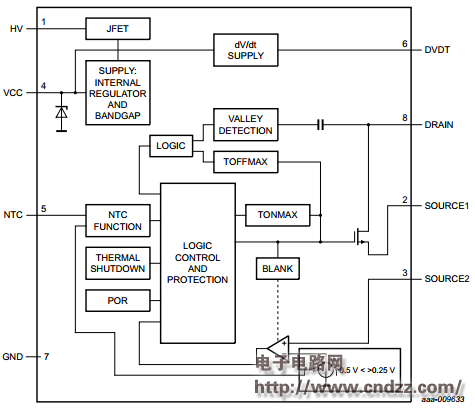
图1SSL5015TE内部结构框图
The SSL5015TE is intended for low-cost mains non-dimmable LED lighting applications, including 18 W T-LEDs or higher power lamps, with a high power factor. The IC operates from 100 V (AC) or 120 V (AC) mains voltages. The output current can be modulated using a PWM signal.
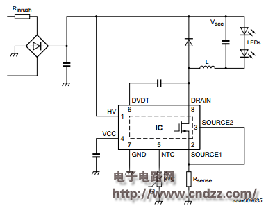
图2SSL5015TE参考设计图
This converter operates at the boundary between continuous and discontinuous modes. Energy is stored in inductor L when the MOSFET is switched on. The inductor current IL is zero when the internal MOSFET is switched on at t0. Thereafter, the amplitude of the current builds up in L proportionally with VIN -VOUT and the time that the internal MOSFET is on (t0 to t1). The peak current sensed at the SOURCE2 pin determines when the MOSFET is switched off. When the internal MOSFET switches off at t1, the current flows through the freewheeling diode and the output capacitor (t2 to t3). The current then drops at a rate proportional to the value of VOUT. When the inductor current reaches zero, after a short delay (t3 to t00), a new switching cycle is started when the MOSFET is switched on again.
SSL5015TE中文数据手册:点击下载
更多原理图及源代码热门应用电路:立刻点击
评论