
TPS65283参考设计电路|同步双路降压转换器应用电路

TPS65283特性:宽幅输入电压范围4.5到18V;反馈基准电压0.6V±1%;外部时钟同步;逐周期电流限制
TPS65283典型应用范围:USB端口和集线器;机顶盒;数字电视;数字用户线路(DSL)/电缆调制解调器,无线路由器;家庭网关和接入点网络
TPS65283参考设计应用电路:
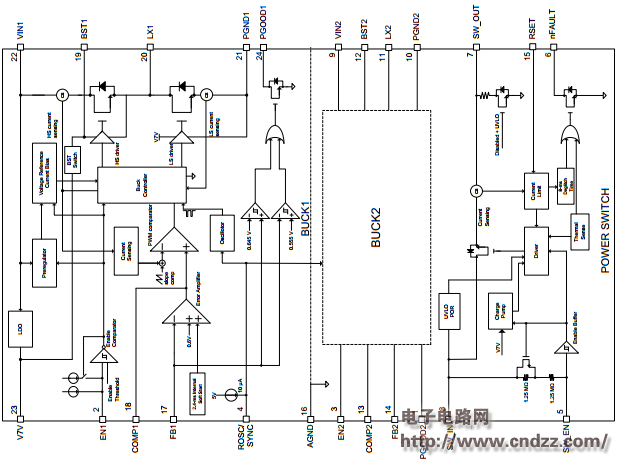
图1TPS65283内部结构图
The TPS65283, TPS65283-1 responds to overcurrent conditions on power switches by limiting the output currents to I OCP_SW level, which is set by external resistor. When the load current is less than the current-limit threshold, the devices are not limiting current. During normal operation, the N-channel MOSFET is fully enhanced, and VSW_OUT = VSW_IN – (ISW_OUT × Rdson_SW).
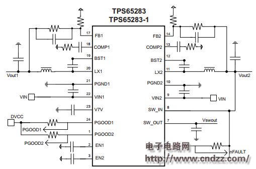
图2TPS65283参考设计图
TheTPS65283, TPS65283-1 in thermally-enhanced 4-mm × 4-mm VQFN package is a full featured 4.5- to 18-V Vin, 3.5-A/2.5-A output current synchronous step down DC-DC converter, which is optimized for small designs through high efficiency and integrating the high-side and low-side MOSFETs.
TPS65283中文数据手册:点击下载
更多原理图及源代码热门应用电路:立刻点击
评论