
MAX1951参考设计电路|DC-DC稳压器应用电路

MAX1951特性:效率高达94%;确保2A的输出电流;工作于2.6V至5.5V电源电压;短路和热过载保护
MAX1951典型应用范围:ASIC/DSP/µP/FPGA核及I/O电压;蜂窝基站;网络与电信系统;机顶盒
MAX1951参考设计应用电路:
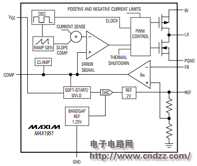
图1MAX1951内部结构图
TheMAX1951/MAX1952 high-efficiency, DC-to-DC step-down switching regulators deliver up to 2A of output current. The devices operate from an input voltage range of 2.6V to 5.5V and provide an output voltage from 0.8V to VIN, making the MAX1951/MAX1952 ideal for on-board postregulation applications. The MAX1951 total output error is less than 1% over load, line, and temperature.
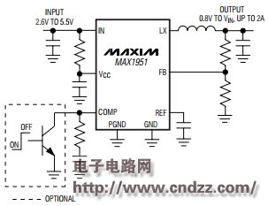
图2MAX1951参考设计图
TheMAX1951/MAX1952 high-efficiency switching regulators are small, simple, DC-to-DC step-down converters capable of delivering up to 2A of output current. The devices operate in pulse-width modulation (PWM) at a fixed frequency of 1MHz from a 2.6V to 5.5V input voltage and provide an output voltage from 0.8V to VIN, making the MAX1951/MAX1952 ideal for on-board postregulation applications.
MAX1951中文数据手册:点击下载
更多原理图及源代码热门应用电路:立刻点击
评论