
Lattice MachXO3L系列非易失性PLD开发方案

Lattice公司的MachXO3L系列是超低密度低功耗PLD,查找表(LUT)从640到6900个,是最先进成本超低的桥接和I/O扩展解决方案,支持SPI、I2C、CSI-2和DSI的MachXO3器件为低成本和现有的微控制器添加瞬时启动的GPIO以及到图像传感器的连接,采用惊人的小尺寸封装2.50 mm x 2.50 mm WLCSP封装和引脚间距为0.50 mm和0.80 mm的BGA封装,具备双引导以及后台升级的1ms瞬时启动,可选1.2V低内核电压或3.3/2.5V内核电压,多达335个IO的高IO-LUT比,支持在现有的设计中添加SPI、I2C、CSI-2和DSI接口以及非易失性,MachXO3L带有可多次编程的NVCM,MachXO3LF支持可无限次重配置的闪存.主要用在消费类电子,无线通信,工业控制系统,汽车电子和计算与存储系统.本文介绍了MachXO3系列主要特性,框图和选型表,MachXO3L入门套件主要功能和主要特性,框图,电路图和材料清单.
MachXO3TM device family is an Ultra-Low Density family that supports the most advanced programmable bridging and IO expansion. It has the breakthrough IO density and the lowest cost per IO. The device IO features have the integrated support for latest industry standard IO. The MachXO3L family of low power, instant-on, non-volatile PLDs has five devices with densities ranging from 640 to 6900 Look-Up Tables (LUTs). In addition to LUT-based, low-cost programmable logic these devices feature Embedded Block RAM (EBR), Distributed RAM, Phase Locked Loops (PLLs), pre-engineered source synchronous I/O support, advanced configuration support including dual-boot capability and hardened versions of commonly used functions such as SPI controller, I2C controller and timer/counter. These features allow these devices to be used in low cost, high volume consumer and system applications. The MachXO3L devices are designed on a 65nm non-volatile low power process. The device architecture has sev-eral features such as programmable low swing differential I/Os and the ability to turn off I/O banks, on-chip PLLs and oscillators dynamically. These features help manage static and dynamic power consumption resulting in low static power for all members of the family.
The MachXO3L devices are available in two versions C and E with two speed grades: -5 and -6, with -6 being the fastest. C devices have an internal linear voltage regulator which supports external VCC supply voltages of 3.3 V or 2.5 V. E devices only accept 1.2 V as the external VCC supply voltage. With the exception of power supply voltage both C and E are functionally compatible with each other. The MachXO3L PLDs are available in a broad range of advanced halogen-free packages ranging from the space saving 2.5 x 2.5 mm WLCSP to the 17 x 17 mm caBGA. MachXO3L devices support density migration within the same package. Table 1-1 shows the LUT densities, package and I/O options, along with other key parameters. The MachXO3L devices offer enhanced I/O features such as drive strength control, slew rate control, PCI compati-bility, bus-keeper latches, pull-up resistors, pull-down resistors, open drain outputs and hot socketing. Pull-up, pull-down and bus-keeper features are controllable on a “per-pin” basis. A user-programmable internal oscillator is included in MachXO3L devices. The clock output from this oscillator may be divided by the timer/counter for use as clock input in functions such as LED control, key-board scanner and sim-ilar state machines. The MachXO3L devices also provide flexible, reliable and secure configuration from on-chip NVCM. These devices can also configure themselves from external SPI Flash or be configured by an external master through the JTAG test access port or through the I2C port. Additionally, MachXO3L devices support dual-boot capability (using exter-nal Flash memory) and remote field upgrade (TransFR) capability. Lattice provides a variety of design tools that allow complex designs to be efficiently implemented using the MachXO3L family of devices. Popular logic synthesis tools provide synthesis library support for MachXO3L. Lattice design tools use the synthesis tool output along with the user-specified preferences and constraints to place and route the design in the MachXO3L device. These tools extract the timing from the routing and back-annotate it into the design for timing verification. Lattice provides many pre-engineered IP (Intellectual Property) LatticeCORE™ modules, including a number of reference designs licensed free of charge, optimized for the MachXO3L PLD family. By using these configurable soft core IP cores as standardized blocks, users are free to concentrate on the unique aspects of their design, increasing their productivity.
MachXO3系列主要特性:
Solutions
• Smallest footprint, lowest power, high data throughput bridging solutions for mobile applications
• Optimized footprint, logic density, IO count, IO performance devices for IO management and logic applications
Flexible Architecture
• Logic Density ranging from 640 to 6.9K LUT4
•High IO to LUT ratio with up to 335 IO pins
Advanced Packaging
• 0.4 mm pitch: 1K to 4K densities in very small footprint WLCSP (2.5 mm x 2.5 mm to 3.8 mm x 3.8 mm) with 28 to 63 IOs
• 0.5 mm pitch: 640 to 6.9K LUT densities in 6 mm x 6 mm to 10 mm x 10 mm BGA packages with up to 281 IOs
•0.8mm pitch: 1K to 6.9K densities with up to 335 IOs in BGA packages
Pre-Engineered Source Synchronous I/O
• DDR registers in I/O cells
• Dedicated gearing logic
• 7:1 Gearing for Display I/Os
High Performance, Flexible I/O Buffer
• Programmable sysIOTM buffer supports wide range of interfaces:
- LVCMOS 3.3/2.5/1.8/1.5/1.2
- LVTTL
- LVDS, Bus-LVDS, MLVDS, LVPECL
- MIPI D-PHY Emulated
- Schmitt trigger inputs, up to 0.5 V hysteresis
• Ideal for IO bridging applications
• I/Os support hot socketing
• On-chip differential termination
• Programmable pull-up or pull-down mode
High Performance, Flexible I/O Buffer
• Programmable sysIOTM buffer supports wide range of interfaces:
• Ideal for IO bridging applications
• I/Os support hot socketing
• On-chip differential termination
• Programmable pull-up or pull-down mode
Flexible On-Chip Clocking
• Eight primary clocks
• Up to two edge clocks for high-speed I/O inter-faces (top and bottom sides only)
• Up to two analog PLLs per device with frac-tional-n frequency synthesis
Non-volatile, Multi-time Programmable
• Instant-on
• Single-chip, secure solution
• Programmable through JTAG, SPI or I2C
TransFR Reconfiguration
•In-field logic update while IO holds the system state
Enhanced System Level Support
• On-chip hardened functions: SPI, I2C, timer/ counter
• On-chip oscillator with 5.5% accuracy
• Unique TraceID for system tracking
• Single power supply with extended operating range
• IEEE Standard 1149.1 boundary scan
• IEEE 1532 compliant in-system programming
MachXO3L应用:
• Consumer Electronics
• Compute and Storage
• Wireless Communications
• Industrial Control Systems
• Automotive System
MachXO3L系列产品选型表:


图1.MachXO系列顶视图

图2.MachXOL-4300顶视图
MachXO3L入门套件
The MachXO3L Starter Kit is a basic breakout board to allow simple evaluation and development of MachXO3L based designs. It has the LCMXO3L-6900C-5BG256C device on it. It is significantly smaller in size and lower cost than the MachXO3L DSI (LCXO3L-DSI-EVN) or SMA (LCXO3L-SMA-EVN) breakout boards while offering common basic functionalities – a good way to start the evaluation of MachXO3L. A SPI Flash is available on this Starter Kit board for evaluating external boot or dual-boot functional capabilities. The MachXO3L DSI breakout board is recommended for MIPI DSI and CSI2 I/O evaluation and the MachXO3L SMA breakout board is recommended for high-speed differential I/O evaluation.
This Starter Kit board is a 3 x 3 inch form factor, and features a USB mini-B connector for power and programming, an LED array, and prototype area. It comes with a pre-loaded demonstration, a counter design that highlights use of the embedded MachXO3L oscillator and programmable I/Os configured for LED drive. A USB cable is also included with the kit, and demos area available for download. By using the free Lattice design tools, you can program the MachXO3L device to review your own custom design.
MachXO3L入门套件主要功能:
Evaluate CMOS I/Os
LED driving capability
Programming via JTAG or I2C
SPI flash for external boot or dual-boot operation
MachXO3L入门套件主要特性:
MachXO3L FPGA – LCMXO3L-6900C-5BG256C
USB Mini-B connector (program/power)
Pre-programmed example design (available on latticesemi.com)
Eight LEDs
4-position DIP switch
40-hole Prototyping area
Four 2 x 20 expansion header landing for general I/O, JTAG and external power
1 x 8 expansion header landing for JTAG
1 x 6 expansion header landing for SPI/ I2C
SPI Flash for external boot or dual boot
3.3 V and 1.2 V supply rails
RoHS-compliant
The MachXO3 Starter Kit includes:
• MachXO3L/LF Board – The board is a 3” x 3” form factor that features the following on-board components and circuits:
— MachXO3 FPGA – LCMXO3L-6900C-5BG256C (NVCM Based) or LCMXO3LF-6900C-5BG256C (Flash Based)
— USB mini-B connector for power and programming
— 4-Mb Serial Flash Memory for boot image and dual-boot support.
— Eight LEDs
— 4-position DIP switch
— Momentary push button switch
— 40-hole prototype area
— Four 2 x 20 expansion header landings for general I/O, JTAG, and external power
— 1 x 8 expansion header landing for JTAG
— 1 x 6 expansion header landing for SPI/I2C
— 3.3 V and 1.2 V supply rails
• Pre-loaded Demo – The kit includes a pre-loaded counter design that highlights use of the embedded MachXO3 oscillator and programmable I/Os configured for LED drive.
• USB Connector Cable – The board is powered from the USB mini-B socket when connected to a host PC. The USB channel also provides a programming interface to the MachXO3 JTAG port.
• Lattice Development Kits and Boards Web Page – Visit www.latticesemi.com/breakoutboards for the latest documentation (including this guide) and drivers for the kit.

图3.MachXO3板(MachXO3L型)外形图(正面)

图4.MachXO3板(MachXO3L型)外形图(背面)
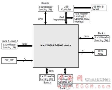
图5.MachXO3L/LF-6900C框图

图6.MachXO3L/LF-6900C电路图(1)
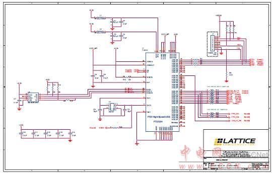
图7.MachXO3L/LF-6900C电路图(2)

图8.MachXO3L/LF-6900C电路图(3)
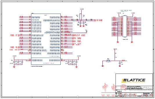
图9.MachXO3L/LF-6900C电路图(4)

图10.MachXO3L/LF-6900C电路图(5)
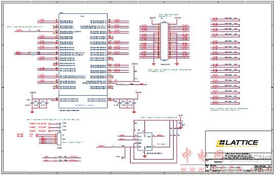
图11.MachXO3L/LF-6900C电路图(6)

图12.MachXO3L/LF-6900C电路图(7)
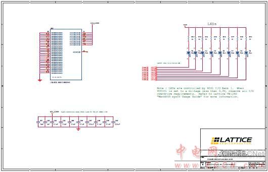
图13.MachXO3L/LF-6900C电路图(8)
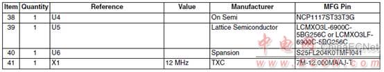
MachXO3L/LF-6900C材料清单:

评论