
在应用编程MAXQ微控制器中可分区擦除的程序和数据闪存

摘要:本应用笔记介绍了MAXQ微控制器中的程序和数据闪存,以及如何使用内置的应用ROM对闪存进行擦/写。本应用笔记适用于所有使用分区擦除闪存的MAXQ微控制器。
引言
本应用笔记介绍了如何管理MAXQ微控制器中、可分区擦除的内部数据和程序闪存。一般性地介绍了怎样构建一个引导装载应用,实现程序闪存的在应用编程。注意:本文不适于那些使用页擦除闪存的MAXQ微控制器,即那些只允许少量闪存被擦除的微控制器。各MAXQ数据手册都会说明其所采用的闪存类型。
闪存简介
存储器配置
本应用笔记给出了多种不同尺寸的闪存配置,并不完全和某一特定MAXQ器件相符。这些配置仅用于本文中的实例。各MAXQ器件的数据手册会列出该器件的存储器配置。
引导、程序和数据区在操作上并没有区别。如果引导装载程序需要的空间超过了第一闪存区的范围,那么可将程序扩展到下一分区中。然而,在下面的实例中,标号会有所不同。
表1. 闪存配置实例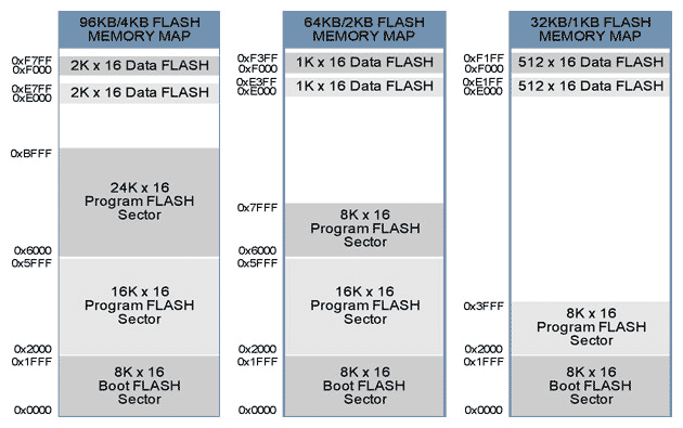
数据闪存
数据闪存可以被用来可靠地存储一些系统工作期间需要一次性或周期性保存的系统数据。数据闪存的容量因特定的MAXQ器件而异,通常在128至2k字之间。
数据闪存的使用有一些限制。与EEPROM不同,数据闪存不能按字擦除;每次必须擦除一个完整的分区。擦除一个分区通常需要0.7秒的时间,最坏情况下可能会长达15秒。在这期间,用户代码停止运行,不能进行其他操作。因此,在根据系统需求选择软件技术时,必须要仔细考虑这些限制。对于绝大多数周期性数据存储,采用有界队列和/或分区切换技术,即可满足系统可靠性的要求。下面给出分区交换和有界队列技术的简单实例。
有界队列
有界队列是一个包含固定数量元素的队列。该方法常用于处理周期性数据。例如,可以将一个2k字的数据闪存分成32至64个字的条目,如表2所示的存储器配置。
初始化时,启动程序扫描队列,以确定队列中下一个可用条目。队列填满之后只有将其擦处后方可写入下一个条目。如果要保留全部条目,那么必须改变分区以保持所有数据。闪存擦除后,则可以写入新的条目。这种方法的缺点是在擦写过程中如果掉电,所有数据将会丢失。图1示例条目载入有界队列的流程。附录A给出了一个简单的C源代码实例。
如果这种有界队列方法还不能满足您的系统要求,那么还可以采用分区交换技术。
表2. 有界队列存储器配置举例
| FLASHQueue[ ] | |
| Queue Index | Data Flash Address |
| 31 | 0xF7C0-0xF7FF |
| 30 | 0xF780-0xF7BF |
| 29 | 0xF740-0xF77F |
| . . . . | . . . . |
| 2 | 0xF080-0xF0BF |
| 1 | 0xF040-0xF07F |
| 0 | 0xF000-0xF03F |
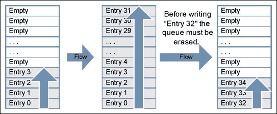
图1. 有界队列流程
块交换
块交换能够有效防止数据在漫长的分区擦除过程中丢失或损坏。这里所讲的“块”等同于“分区”。块交换方式最适合于分区尺寸略大于数据总量的情况。缺点是至少需要两个数据闪存分区。当要写入的数据总量远小于分区尺寸时,最好将块交换和有界队列两种方法结合使用。
如果需要采用块交换,则需要选用至少含有两个数据闪存分区的MAXQ器件。表3给出了一个包含两个1K x 16闪存分区的存储器配置实例。图2给出了块交换写/擦流程。
附录A给出了一个简单的C源代码实例。
表3. 块交换存储器配置实例
| Flash Sectors | |
| Sector Number | Data Flash Address |
| 0 | 0xF000-0xF3FF |
| 1 | 0xE000-0xE3FF |
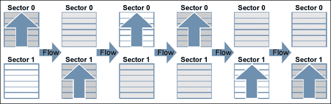
图2. 块交换流程
同时采用有界队列和块交换
管理数据闪存的最可靠、最灵活的办法是同时采用有界队列和块交换技术。当需要将少量的数据周期性存入闪存,并要保持数据完整性的时候,结合使用这两种技术将非常有利。表4给出了一个包含两个2K x 16分区,每个分区被划分为32个相等条目的实例。图3示例数据在两个分区之间、有界排队内的流向。
这种组合方法的程序比有界队列方法稍微复杂一些。附录A给出了一个简单的C源代码实例。
表4. 块交换和有界队列存储器配置实例
| FQueueBank0[ ] | |
| Queue Index | Data Flash Address |
| 31 | 0xF7C0-0xF7FF |
| 30 | 0xF780-0xF7BF |
| 29 | 0xF740-0xF77F |
| . . . . | . . . . |
| 2 | 0xF080-0xF0BF |
| 1 | 0xF040-0xF07F |
| 0 | 0xF000-0xF03F |
| FQueueBank0[ ] | |
| Queue Index | Data Flash Address |
| 31 | 0xE7C0-0xE7FF |
| 30 | 0xE780-0xE7BF |
| 29 | 0xE740-0xE77F |
| . . . . | . . . . |
| 2 | 0xE080-0xE0BF |
| 1 | 0xE040-0xE07F |
| 0 | 0xE000-0xE03F |
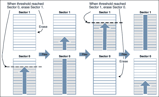
图3. 有界队列和块交换流程
应用ROM闪存例程
MAXQ微控制器具有片内闪存支持程序,驻留在ROM (只读内存)中,用来对闪存进行编程、擦写和校验。有两种方法来调用这些例程。第一种也是最快的方法是直接访问,只需通过以下代码提供一个头文件:
u16 flashEraseSector(void *)
;u16 flashEraseAll(void)
;u16 flashWrite(u16 *pAddress, u16 iData);
然后,加入链接定义给每个例程分配合适的地址。对于IAR链接文件,加入下面几行语句:
-DflashEraseSector=0x8XXX-DflashEraseAll=0x8XXX-DflashWrite=0x8XXX
具体使用时,用每个例程相应的存储器地址替代0x8XXX。其他编译器可能使用不同的方法添加这些声明。
注意,直接访问方法与未来的ROM版本无法前向兼容。
第二种为查表法。尽管这种方法兼容性较好,但是执行时间较长。在下面每一段例程说明的后面,汇编例程采用查表法获取ROM应用例程的地址。表5所示为应用ROM提供的几个闪存例程。关于ROM应用例程的完整列表,参见特定MAXQ器件的用户指南。
表5. 应用ROM闪存例程
| RouTIne Number | RouTIne Name | Entry Point ROMTable = ROM[800Dh] | Entry Point Physical Address |
| 2 | flashEraseSector | ROM[ROMTable + 1] | 0x8XXX |
| 3 | flashEraseAll | ROM[ROMTable + 2] | 0x8XXX |
| 15 | flashWrite | ROM[ROMTable + 14] | 0x8XXX |
flashWrite
| RouTIne | u16 flashWrite(u16 *pAddress, u16 iData) |
| Summary | Programs a single word of flash memory. |
| Inputs | A[0] - Word address in flash memory to which to write. A[1] - Word value to write to flash memory. |
| Outputs | Carry: Set on error and cleared on success. If set, then A[0] contains one of the following error codes: 1 : failure due to software TImeout 2 : failure reported by hardware (DQ5/FERR) 4 : command not supportedSW_FERR - Set on error, cleared on success. |
| Notes | The watchdog must not be active, or the watchdog timeout must be set long enough to complete this routine without triggering a reset. |
以下汇编代码实例采用间接寻址方法(查表)调用flashWrite()应用例程。该例程可由C代码调用。
; This routine is callable by C code using the following prototype
; u16 flashWrite(u16 *pAddress, u16 iData);
;flashWrite:move APC, #0
; No auto inc/dec of accumulator.move AP,  #2
; Set ACC to A[2]move DP[0], #0800Dh
; This is where the address of the table is stored.move ACC, @DP[0]
; Get the location of the routine table.add  #14
; Add the index to the flashWrite routine.move DP[0], ACCmove ACC, @DP[0]
; Retrieve the address of the routine.call ACC
; Execute the routine.ret
; Status returned in A[0]
flashEraseSector
| Routine | u16 flashEraseSector(void *pAddress) |
| Summary | Erases a single sector of flash memory |
| Inputs | A[0] - Address located in the sector to erase. |
| Outputs | Carry: Set on error and cleared on success. If set, then A[0] contains one of the following error codes: 1 : failure due to software timeout 2 : failure reported by hardware (DQ5/FERR) 4 : command not supported SW_FERR - Set on error, cleared on success. |
| Notes | The watchdog must not be active, or the watchdog timeout must be set long enough to complete this routine without triggering a reset. |
; This routine is callable by C code using the following prototype
; u16 flashEraseSector(void *pAddress);
;flashEraseSector:move APC, #0
; No auto inc/dec of accumulator.move AP,  #1
; Set ACC to A[1]move DP[0], #0800Dh
; This is where the address of the table is stored.move ACC, @DP[0]
; Get the location of the routine table.add  #1
; Add the index to the flashEraseSector routine.move DP[0], ACCmove ACC, @DP[0]
; Retrieve the address of the routine.call ACC
; Execute the routine.ret
; Status returned in A[0]
flashEraseAll
| Routine | void flashEraseAll(void) |
| Summary | Erases the entire program and data flash memory, including the boot loader sector. This routine is not normally used for IAP, as great care must be taken to ensure that the erase/programming sequence is not interrupted. |
| Inputs | None |
| Outputs | Carry: Set on error and cleared on success.SW_FERR: Set on error, cleared on success. |
| Notes | The watchdog must not be active, or the watchdog timeout must be set long enough to complete this routine without triggering a reset. |
; This routine is callable by C code using the following prototype
; void flashEraseAll(void);;flashEraseAll:move APC, #0
; No auto inc/dec of accumulator.move AP,  #0
; Set ACC to A[0]move DP[0], #0800Dh
; This is where the address of the table is stored.move ACC, @DP[0]
; Get the location of the routine table.add  #2
; Add the index to the flashEraseAll routine.move DP[0], ACCmove ACC, @DP[0]
; Retrieve the address of the routine.call ACC
; Execute the routine.ret
在应用编程
大多数基于闪存的系统要求,当系统安装到终端产品上以后,其固件必须具备升级的能力。这种功能称为在应用编程(IAP)。本节概述了创建一个IAP应用程序的要领。
上面列出的应用ROM闪存例程,可完成闪存ROM所需要的所有擦除和写入操作,从而允许用户代码对闪存进行操作。与其他子程序调用相似,程序执行完成之后,控制将返回到用户代码。
要实现可靠的IAP,引导装载程序必须与主程序分开。这样可以确保在经历一次未竟编程之后,可以重新启动编程过程。
引导装载程序
初始化以后,由于ROM跳转至地址0x0000,因此,引导装载程序的入口应为0x0000。不同的MAXQ器件,其引导闪存分区的大小也不相同。可以根据需要,将引导程序扩展至多个闪存分区,用户应用程序代码不能使用已被占用的任何分区。擦除和写入闪存时必须满足的特定要求见表6。
表6. 调用应用ROM闪存例程的要求
| You cannot erase or program from the same flash sector from which you are executing code. This is not normally a problem since the flash Boot Sector should never be erased during IAP. |
| The watchdog must not be enabled or the watchdog timeout must be set long enough to complete this routine without triggering a reset before the flashEraseSector() routine is called. If the watchdog time out occurs before the erase is complete, it will reset the part. Erasing a sector typically takes 0.7 seconds; it can take up to 15 seconds under worst case conditions. |
| Since the System Control Register bit SC.UPA must be set to 0 to access the Utility ROM, a ROM Utility routine cannot be called directly from program memory addresses = 0x8000. If access to a Utility ROM routine is required from a program in upper memory (= 0x8000), the program must indirectly call the ROM routine through a routine residing in lower memory (<0x8000). This effectively limits the boot loader to = 64kB (32kB x 16). |
图4中的流程说明了脱离复位状态后MAXQ的操作。ROM进行自诊断并确定闪存已经准备好以后,ROM初始化代码直接跳转到地址0x0000。请阅读相关的数据手册和用户指南,确定您的MAXQ微控制器是否按照这个启动顺序运行。
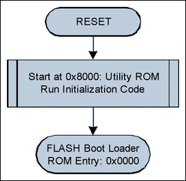
图4. ROM初始化流程示意
图5给出了一个简单的引导装载程序的流程图。当使用引导装载程序实现IAP时,对于16kB (8K x 16)的引导装载程序,主应用程序的入口通常位于地址0x2000 + 标题偏移,对于32kB (16K x 16)的引导装载程序,则位于地址0x4000 + 标题偏移。一个简单的应用程序标题如下所示:
typedef struct {u16 iSize
;  // The size of the application in wordsu32 iCRC
;   // The CRC of the applicationu8 ID[8]
;   // ID string for current application} APPLICATION_HEADER;
引导装载程序可以利用此标题所提供的信息确定主程序的有效性,如果需要,还可以报告其版本标识。

图5. 闪存引导装载流程示意图
编程过程本身非常简单。首先调用flashEraseSector(),擦除含有主程序代码的每个分区。然后调用flashWrite()逐字写入要编程的代码字。应最先擦除含有应用程序标题的块,而最后编程CRC数据,以便将出现错误CRC匹配的概率降到最低。下面给出通过串口获取数据来刷新微控制器的一个简单例程:
/*
// VerySimpleReFlash()
//    As simple as it gets.
//    Step 1. Wait for erase command, then erase flash.
//    Step 2. Wait for program command, then program flash one word
//            at a time.
*/
void VerySimpleReFlash(){u16 iStatus;
 // The status returned from flash utility ROM callsu16 iSize;
 // The size of the main code to programu16 *pAddress = 0x2000;
 // The starting address of the main applicationInitializeCOMM();
 // Can be CAN or UARTWaitForEraseCommand();SlowDownWatchdog();
 // If watchdog enabled set update > 15siStatus = flashEraseSector(C_ADDRESS_SECTOR_1);
 if (iStatus == 0)iStatus = flashEraseSector(C_ADDRESS_SECTOR_2);
 UpdateWatchdog();
 // Prevent watchdog timeoutSendFlashErasedResponse(iStatus);
 if (iStatus)ResetMicro();
 iSize = WaitForProgramCommand();
 while (iSize--){
 u16 iData = GetWordFromCOMM();
 iStatus = flashWrite(pAddress, iData);
 if (iStatus)break;
 ++pAddress;
 UpdateWatchdog();
 // Prevent watchdog timeout
 }SendFlashWriteResponse(iStatus);
 ResetMicro();
 }
那些引导装载程序没有使用的程序空间,可用于其他例程和/或常数的存储。一个很好的例子是将间接调用应用ROM例程的所有子程序保存在这里,例如上面“应用ROM闪存例程”中所给出的一些子程序。在引导程序分区存储其他信息时需要注意:除非部分或全部擦除引导装载程序自身,否则无法将其擦除。
采用基于RAM的闪存例程实现IAP
当不要求故障恢复时,可采用基于RAM的闪存例程来刷新MAXQ微控制器。该方法要求主程序拷贝一个小的、可再定位的闪存编程例程到RAM中,然后再跳转到该例程。表7列出了从RAM中执行代码需要注意的几个限制。
表7. 从RAM中执行代码的限制
| SC.UPA must be set to 0 before executing a RAM-based routine. This means that the application must jump to the RAM routine from the code segments P0 & P1. |
| RAM cannot be accessed as data and program at the same time. This means that only the registers and hardware stack are available for data storage. |
| The Interrupt Vector must point to a RAM routine if interrupts are enabled. Typically interrupts are turned off and polling is used due to the simplicity of the RAM reflash routine. |
闪存例程一般通过UART或者CAN接口来进行通信。为实现更可靠的错误恢复机制,最好是接收小的数据包,并发送某种类型的确认信息。图6给出了一个更新例程。记住,在掉电之前,如果没有成功完成重新编程,需要通过JTAG端口对微控制器重新编程。
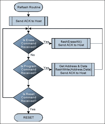
图6. 简化的RAM更新例程流程图

评论