
AKM AK4558 32位数字音频系统CODEC解决方案

AKM公司的AK4558是低电压32位216kHz数字音频系统编译码器(CODEC),支持各种信号,具有较好的带外噪音和低功耗,主要用在高档音响设备和电子乐器以及音频接口.本文介绍了AK4558主要特性和框图,系统连接框图以及评估板AKD4558-A功能,框图,电路图和PCB元件布局图.
The AK4558 is a low voltage 32bit 216kHz CODEC for high performance battery powered digital audiosubsystems. An internal circuit includes newly developed 32-bit Digital Filter achieving short group delayand high quality sound. In addition, “OSR-Doubler” technology is newly adopted, making the AK4558capable of supporting wide range signals and achieving low out-of-band noise while realizing low powerconsumption. The AK4558 is ideal for a wide range of applications that demands high sound qualityincluding Electronic musical instruments and Audio Interfaces. The analog inputs and outputs aresingle-ended to minimize pin count and external filtering requirements. The AK4558 is housed in a verysmall 28-pin QFN. It is ideal for space-sensitive applications.
AK4558主要特性:
Single-ended ADC
- Dynamic Range, S/N: 108dB@AVDD=3.3V
- S/(N+D): 92dB@AVDD=3.3V
- Selectable HPF for DC-offset cancel (fc = 1Hz @ fs=48kHz)
- 4-types Digital Filter for High Sound Quality
Single-ended DAC
- Dynamic Range, S/N: 108dB@AVDD=3.3V
- S/(N+D): 100dB@AVDD=3.3V
- Digital de-emphasis for 32kHz, 44.1kHz and 48kHz sampling
- 5-types Digital Filter for High Sound Quality
- Channel Independent Digital Attenuator (256 levels, 0.5dB steps)
Audio I/F format: MSB First, 2’s Complement
- ADC: 24/32bit MSB justified , 24/32bit I2S compatible or TDM
- DAC: 24/32bit MSB justified, 16/20/24/32bit LSB justified,
24/32bit I2S compatible or TDM
Input/Output Voltage: ADC = 2.64Vpp @ AVDD=3.3V
DAC = 2.51Vpp @ AVDD=3.3V
Master/Slave mode
P I/F: I2C Bus
Sampling Rate:
(1) PLL Mode
• PLL Slave Mode (LRCK pin): fs = 8kHz 216kHz
• PLL Slave Mode (BICK pin): fs = 8kHz 216kHz
• PLL Master Mode: 8kHz, 11.025kHz, 12kHz, 16kHz, 22.05kHz, 24kHz, 32kHz,44.1kHz,
48kHz,54kHz,88.2kHz,96kHz,128kHz,176.4kHz,192kHz
(2) External Clock Mode
• Normal Speed: 8kHz to 54kHz (256fs or 512fs)
8kHz to 48kHz (384fs or 768fs)
• Double Speed: 54kHz to 108kHz (256fs)
48kHz to 96kHz (384fs)
• Quad Speed: 108kHz to 216kHz (128fs)
96kHz to 192kHz (192fs)
Master Clock:
(1) PLL Mode
• MCKI pin: 27MHz, 26MHz, 24MHz, 19.2MHz, 13.5MHz, 13MHz, 12.288MHz, 12MHz,
11.2896MHz
• LRCK pin: 1fs
• BICK pin: 32fs, 64fs, 128fs(TDM), 256fs(TDM)
(2) External Clock Mode (MCKI pin)
• Slave mode: 256fs, 384fs, 512fs or 768fs (Normal Speed)
256fs or 384fs (Double Speed)
128fs or 192fs (Quad Speed)
• Master mode: 256fs or 512fs (Normal Speed)
256fs (Double Speed)
128fs (Quad Speed)
Power Supply:
• AVDD = 2.4 to 3.6V (typ. 3.3V)
• TVDD = 1.7 to 3.6V (typ. 1.8V)
Power Supply Current: 18mA(fs=48kHz)
Ta = -40 to 105℃
Package: 28-pin QFN (0.5mm pitch)
.jpg")
图1. AK4558框图
.jpg")
图2. AK4558系统连接框图(PS pin= “H”, LDOE pin= “H”)
.jpg")
图3. AK4558系统连接框图(PS pin= “L”, LDOE pin= “L”)
AK4558评估板AKD4558-A
The AKD4558-A is an evaluation board for AK4558, which is 24/32bit, CODEC including 2ch ADC and2ch DAC. The control settings of this board may be controlled via USB port, allowing for easy A/D andD/A evaluation. BNC connectors are used for the input and output of the analog signals. This board alsohas a digital interface which can be connected to the digital audio system via optical connector.
评估板AKD4558-A功能:
Clock generator circuit (AK4118A used)
Compatible with 2types of digital audio interface
- Optical input (x1) / Optical output (x1)
- Pin header for external data source
BNC connector for an external clock input
ADC 2ch input, DAC 2ch output
USB port and 10pin header for board control
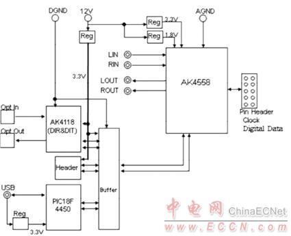
图4.评估板AKD4558-A框图
.jpg")
图5.评估板AKD4558-A板框图
主要元件描述:
(1) U1 ( AK4558 )
24/32bit,2ch A/D Converter, 2ch D/A Converter.
(2) J200, J201, J202, J203 ( Analog data )
J200, J201 BNC connector : Analog Input for LIN, RIN.
J202, J203 BNC connector : Analog Output for LOUT, ROUT.
(3) PORT1, PORT2 ( Optical Connector )
PORT1 : Input optical signal to AK4118A.
PORT2 : Output optical signal from AK4118A.
(4) J700, J701, J702, J703, J704, J705, J706 ( Power supply )
J700 (+12V) : +12V Power Supply
J701 (AVDD1), J704 (D3.3V) : 3.3V Power Supply
J702 (TVDD) : 1.8V/3.3V Power Supply
J703 (VDD18) : 1.8V Power Supply
J705 (AVSS), J706 (DGND) : GND
(5) U2 ( AK4118A )
AK4118A has DIR, DIT and X’tal oscillator.
Transports input data to AK4558 when working in master mode, and output data from AK4558 when working inslave mode.
(6) U60 ( PIC18F4550 )
USB control chip. Sets up AK4558 registers from PC via USB port (PORT600).
(7) J400 (BNC Connector)
Input external clock source.
(8) SW300 ( Dip-switch )
DIP type switch. Sets clock and audio format of AK4118A. DIF[2:0] used to set audio interface format and
OCKS[1:0] used to master clock frequency.
(9) SW500, SW501 ( Dip-switch )
DIP type switch. Sets clock and audio format and filter of AK4558.
(10)SW400 ( Toggle switch )
Toggle type-switch PDN for AK4558.
“H” : PDN = High
“L” : PDN = Low
(11)SW401 ( Toggle switch )
Toggle type-switch PDN for AK4118A.
“H” : PDN = High
“L” : PDN = Low
(12)T1, T2, T3 ( regulator )
Regulator for AK4558, AK4118A, Logic Circuit.
T1 : Regulated AVDD1, TVDD (3.3V) from +12V.
T2 : Regulated TVDD, VDD18 (1.8V) from +12V.
T3 : Regulated D3.3V (3.3V) from +12V.
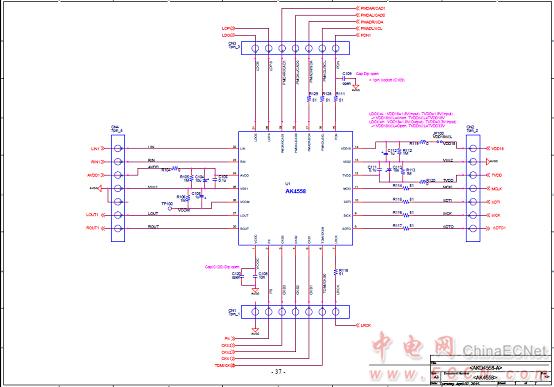
图6.评估板AKD4558-A电路图(1)
.jpg")
图7.评估板AKD4558-A电路图(2)
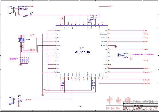
图8.评估板AKD4558-A电路图(3)
.jpg")
图9.评估板AKD4558-A电路图(4)
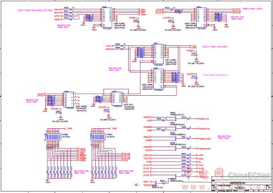
图10.评估板AKD4558-A电路图(5)
.jpg")
图11.评估板AKD4558-A电路图(6)
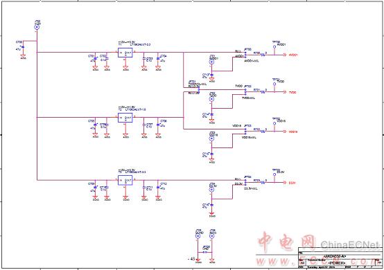
图12.评估板AKD4558-A电路图(7)
.jpg")
图13.评估板AKD4558-A PCB元件布局图(顶层)
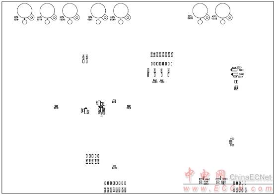
图14.评估板AKD4558-A PCB元件布局图(底层)
.jpg")
图15.评估板AKD4558-A PCB布局图(1)

图16.评估板AKD4558-A PCB布局图(2)
评论