Renesas RL78L1C 16位MCU开发方案


Renesas公司的RL78L1C是16位单片MCU,内置了LCD驱动器和US 2.0功能,支持三种LCD驱动电压产生方法.器件采用RL78-S3内核,三级流水线CISC哈佛架构,具有高性别能和高度功能指令处理,寻址空间1MB,单电压1.6-3.6V工作,主要用在传感器模块,健康设备,家用电器和测量设备.本文介绍了RL78/L1C主要特性,框图, RL78/L1C入门开发板主要特性,框图,主要元件分布图和CPU板电路图.
RL78/L1C microcontrollers have a built-in segment LCD driver and USB 2.0 function. Three LCD driving voltage generation methods (external resistance division, capacitive split, and internal voltage boost) are supported, corresponding to a variety of segment LCD panels. They realize low current consumption (*1): external resistance division: 1.76 μA (*2), internal voltage boost: 1.23 μA, and capacitive split: 0.74 µA. They support USB high-speed battery charging (Battery Charging Specification 1.2) and come in a lineup of 80/100-pin, maximum 416 segment products. These microcontrollers can be used in sensor modules and healthcare devices as well as home appliances and measurement devices.
The CPU core in the RL78 microcontroller employs the Harvard architecture which has independent instruction fetchbus, address bus and data bus. In addition, through the adoption of three-stage pipeline control of fetch, decode, and memory access, the operation efficiency is remarkably improved over the conventional CPU core. The CPU core features high performance and highly functional instruction processing, and can be suited for use in various applications that require high speed and highly functional processing.
The RL78/L1C integrates the RL78-S3 core that has the following features.
• 3-stage pipeline CISC architecture
• Address space: 1 Mbyte
• Minimum instruction execution time: One instruction per clock cycle
• General-purpose registers: Eight 8-bit registers
• Type of instruction: 81
• Data allocation: Little endian
• Multiply/divide and multiply/accumulate instructions: Supported
RL78/L1C主要特性:
Ultra-low power consumption technology
• VDD = single power supply voltage of 1.6 to 3.6 V
• HALT mode
• STOP mode
• SNOOZE mode
RL78 CPU core
• CISC architecture with 3-stage pipeline
• Minimum instruction execution time: Can be changed from high speed (0.04167us: @ 24 MHz operation with high-speed on-chip oscillator clock or PLL clock) to ultra-low speed (30.5us: @ 32.768 kHz operation with subsystem clock)
• Multiply/divide and multiply/accumulate instructions are supported.
• Address space: 1 Mbyte
• General-purpose registers: (8-bit register 8) 4 banks
• On-chip RAM: 8 to 16 KB
Code flash memory
• Code flash memory: 64 to 256 KB
• Block size: 1 KB
• Prohibition of block erase and rewriting (security function)
• On-chip debug function
• Self-programming (with boot swap function/flash shield window function)
Data flash memory
• Data flash memory: 8 KB
• Background operation (BGO): Instructions can be executed from the program memory while rewriting the data flash memory.
• Number of rewrites: 1,000,000 times (TYP.)
• Voltage of rewrites: VDD = 1.8 to 3.6 V
High-speed on-chip oscillator
• Select from 48 MHz, 24 MHz, 16 MHz, 12 MHz, 8 MHz, 6 MHz, 4 MHz, 3 MHz, 2 MHz, and 1 MHz
• High accuracy: ±1.0% (VDD = 1.8 to 3.6 V, TA = -20 to +85 C)
Operating ambient temperature
• TA = -40 to +85 C (A: Consumer applications)
• TA = -40 to +105 C (G: Industrial applications)
Power management and reset function
• On-chip power-on-reset (POR) circuit
• On-chip voltage detector (LVD) (Select interrupt and reset from 12 levels)
Data transfer controller (DTC)
• Transfer modes: Normal transfer mode, repeat transfer mode, block transfer mode
• Activation sources: Activated by interrupt sources (30 to 33 sources).
• Chain transfer function
Event link controller (ELC)
• Event signals of 30 or 31 types can be linked to the specified peripheral function.
Serial interfaces
• CSI: 4 channels
• UART/UART (LIN-bus supported): 4 channels
• I2C/simplified I2C: 5 channels
Timers
• 16-bit timer: 11 channels
• 12-bit interval timer: 1 channel
• Real-time clock 2: 1 channel (calendar for 99 years, alarm function, and clock correction
function)
• Watchdog timer: 1 channel (operable with the dedicated low-speed on-chip oscillator)
LCD controller/driver
• Internal voltage boosting method, capacitor split method, and external resistance division method are switchable.
• Segment signal output: 44 (40) Note 1 to 56 (52)
• Common signal output: 4 (8)
USB
• USB version 2.0 (function controller)
• Full-speed transfer (12 Mbps) and low-speed transfer (1.5 Mbps) are supported
• Compliant to Battery Charging Specification Revision 1.2
A/D converter
• 8/10-bit resolution A/D converter (VDD = 1.6 to 3.6 V)
• 12-bit resolution A/D converter (VDD = 2.4 to 3.6 V)
• Analog input: 9 to 13 channels
• Internal reference voltage (TYP. 1.45 V) and temperature sensor
D/A converter
• 8-bit resolution D/A converter (VDD = 1.6 to 3.6 V)
• Analog output: 2 channels
• Output voltage: 0 V to VDD
• Real-time output function
Comparator
• 2 channels
• Operating modes: Comparator high-speed mode, comparator low-speed mode, window mode
• The external reference voltage or internal reference voltage can be selected as the reference voltage.
I/O ports
• I/O ports: 59 to 77 (N-ch open drain I/O [withstand voltage of 6 V]: 2)
• Can be set to N-ch open drain, TTL input buffer, and on-chip pull-up resistor
• On-chip key interrupt function
• On-chip clock output/buzzer output controller
Others
• On-chip BCD (binary-coded decimal) correction circuit
RL78/L1C主要应用:
Sensors or measuring instruments for consumer and industry use (Thermostat, Gas detector etc.)
Consumer mobile devices and portable devices
Healthcare devices

图1. RL78/L1C框图(80/85引脚带USB)

图2. RL78/L1C框图(80/85引脚不带USB)

图3. RL78/L1C框图(100引脚带USB)
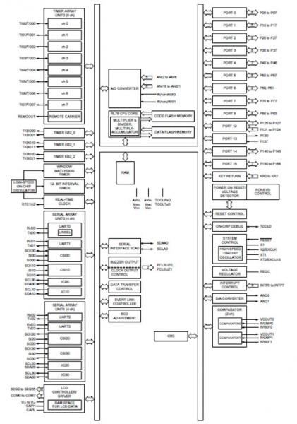
图4. RL78/L1C框图(100引脚不带USB)
RL78/L1C入门开发板
The Renesas Starter Kit for RL78/L1C is intended as a user-friendly introductory and evaluation tool for the RL78/L1C microcontroller. The board also provides a useful platform for evaluating the Renesas suite of development tools for coding and debugging, using CubeSuite+ as well as programming the device using E1 emulator and/or Renesas Flash Programmer.
The Renesas Starter Kit for RL78/L1C may be connected to the host PC using the included USB E1 on chip debugging interface.
The purpose of the board is to enable the user to evaluate the capabilities of the device and its peripherals by giving the user a simple platform on which code can be run only minutes from opening box. It can also prove an invaluable tool in development by providing a useful test platform for code already debugged using one of our more powerful emulation tools.
RL78/L1C入门开发板主要特性:
• Renesas microcontroller programming
• User code debugging
• User circuitry such as switches, LEDs and a potentiometer
• Sample application
• Sample peripheral device initialisation code

图5. RL78/L1C入门开发板外形图
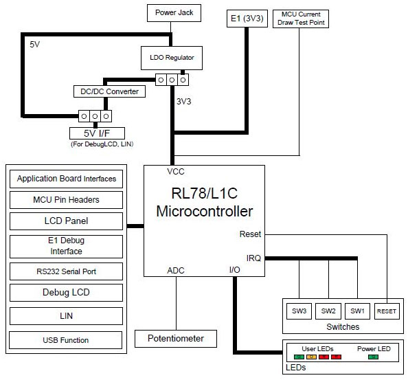
图6. RL78/L1C入门开发板框图

图7. RL78/L1C入门开发板顶层元件分布图
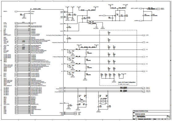
图8. RL78/L1C入门开发板CPU板电路图(1)
.jpg")
图9. RL78/L1C入门开发板CPU板电路图(2)
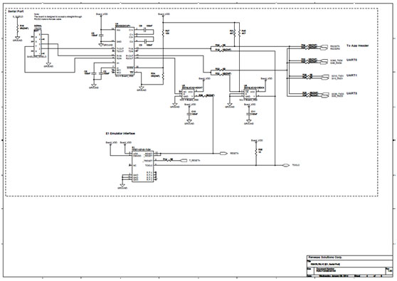
图10. RL78/L1C入门开发板CPU板电路图(3)

图11. RL78/L1C入门开发板CPU板电路图(4
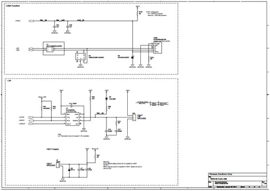
图12. RL78/L1C入门开发板CPU板电路图(5)

图13. RL78/L1C入门开发板CPU板电路图(6)
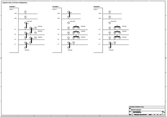
图14. RL78/L1C入门开发板CPU板电路图(7)
评论