
光印电路板制作过程-----pcb making

本文来自下面的连接:http://www.turbokeu.com/myprojects/pcb.htm
本文为国外朋友写的光印电路板的制作过程,这种板子10年前就有了,想想当年拜托别人将电路板文件打印到胶片时别人都不答应,收费也贵,主要是当时激光打印机太贵了,那时候光印电路板价格也贵,现在不知道价格是多少了,因为好久都没有用了,现在主要采用热转印,当然,光印也有自己的优点,就是制作方便,而且做出来的效果也相当不错,就是成本偏贵,有些偏远地方有可能买不到光印电路板。况且如果只制作一次,那么胶片就只用一次,这样我是觉得有点浪费胶片。
制作过程相当简单,将电路板图打印到胶片上,可以先不管正反面,(严格意义上做的话要讲究正反面,因为如果正反面不对的话,在做很细线条的时候效果不好。),在暴光时候别将正反面错了,因为如果正反面弄错了就相当麻烦了。暴光时间大概是8分钟左右就可以了,一般的光印电路板上都有说明要求。显影的时候注意溶液浓度,千万别过度显影了。
本文介绍的腐蚀方法是三氯化铁,我觉得这个容易因为比较黑,不容易看清楚,最好还是使用双氧水与盐酸配置,但是要注意浓盐酸有挥发性,要注意通风。
In answer to the frequently asked question about how I make my Printed Circuit Boards (PCB’s)
I make almost professionally looking PCB’s since years, the only thing I can’t do by myself is the silkscreen mask.
The basic PCB material I use is presensibilized with a UV sensible lacquer (available in most electronic stores).
You can also use non presensibilized PCB material and treat it with Positiv20 spray from Kontakt Chemie. De-oxidate and de-grease the raw PCB material with steel wool and aceton. Atomise a FINE layer of Positiv20 onto the copper and let the PCB dry for 24 hours in ambient room temperature, or about an hour at a maximum of 70°C (do not exceed! ). I do this inmy hot air electric oven in the kitchen.
The drying MUST be done in complete darkness! After that the PCB can be used as normal presensibilized PCB.
All you need is:
- A software to develop your PCB layouts. I use the demo version of Circad’98 from Holophase because of its ease of use.
I also recently bought the cheap Sprint-Layout software from Abacom.
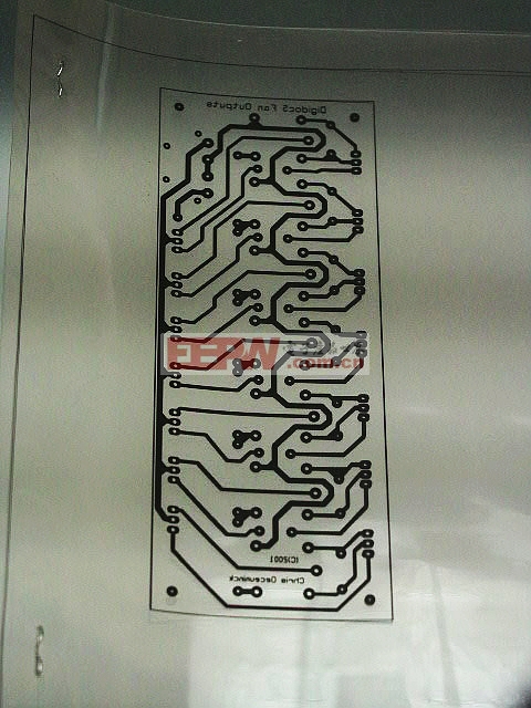
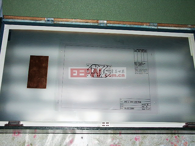
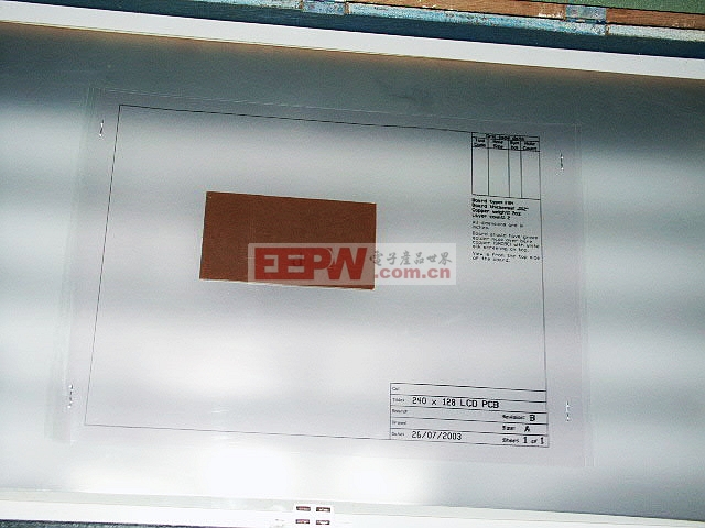
- (Preferably) A laserprinter to print the darkest possible printouts of your PCB layout on transparent slides.
Ialways print out two identical and mirrored slides,so that the tonerside of the upper slide will be in direct contact with the UV-sensible lacquer side of the PCB material(against parasitic UV light between slide and lacquer), and staple themvery precisely together.
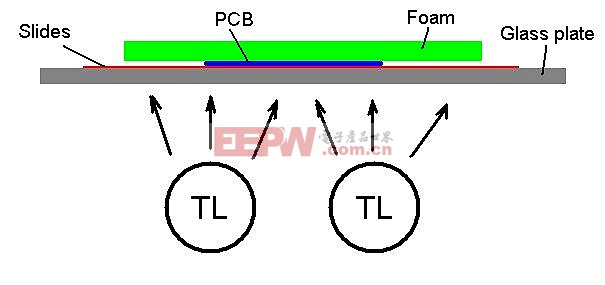
- A UV-exposure unit to expose the PCB material to (short wave) UV light.
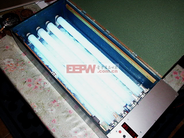
The optimal wave length should be between 370 and 440 nm, withmy Sylvania 350 blacklights that output their peak wave length at 356 nm, it works just fine. Beware these are no blacklights as we know from dancingclubs or case modding, the lamp is just white coated as any other TL lamp when it’s powered off. Powered on it emits a clear blue-ish light (very bad for your eyes!).
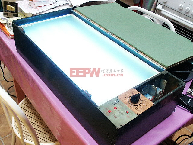
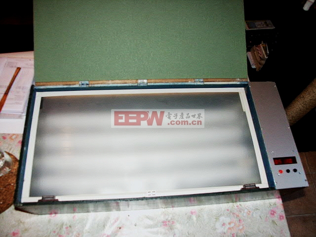
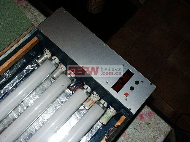
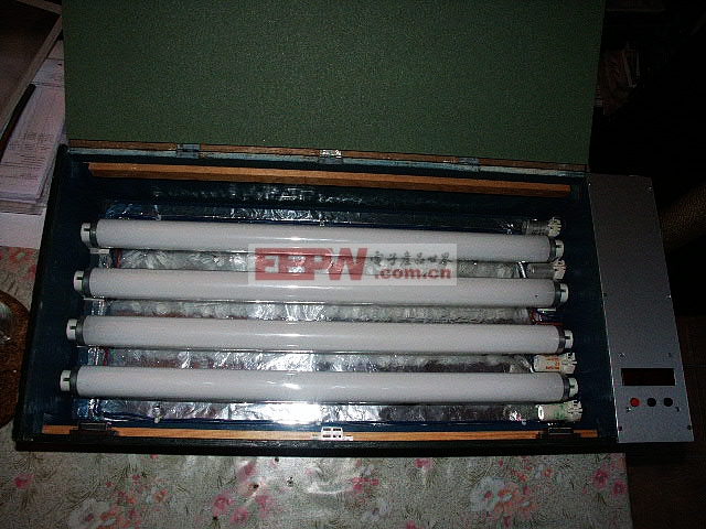
This is my DIY UV-exposure unit, equipped with 4x 20W TL tubes (the unit isalmost 20 years old now!).
In the meanwhile the timer on the picture has been replaced by my DIY microcontroller based timer.
The same results can be obtained with two tubes of 8 or 15W, only exposure timings will be longer.
Also, do not forget to preheat the lamps during 10 minutes to obtain their maximum light output.
To determine the "best" exposure time for the UV exposure I did the following:
- Take a slide with a PCB layout.
- Put a piece of cardboard on 9/10 of the surface.
- Expose for 1 minute.
- Move the cardboard to 8/10 of the surface.
- Expose for 1 more minute.
- Move the cardboard to 7/10 of the surface.
- Expose for 1 more minute. And so on...
- Develop the exposed PCB.
- Examine the results and decide for the best exposure time.
In my case the best exposure time is between 5 and 6 minutes, so I decided for 5min 30secs. I didn’t fail any PCB since then...
- A "tupperware " container to develop the exposed PCB.
After exposure the PCB has to be developed in a solution of sodiumhydroxide (NaOH + water).
Sodiumhydroxide under the form of pellets or flakes is also called caustic soda.
Pre-packaged bags of sodiumhydroxide to dilute in 1 liter of warm tapwater are available at most electronic stores. (I tried with caustic soda and water but it didn’t work out very well...I’ve found that either all or none of the lacquer dissolves)
Pour it into a "tupperware" container big enough to hold the PCB so that the developer is shallow.
You can see the PCB developing (the developer goes blue as soon as the exposed lacquer is dissolving) and the drawing of the layout will become clearly visible on the copper.
Rinse the PCB under flowing tapwater.
The development should be finished within a minute (typically about 30 seconds at 20-25°C) After more than a few minutes the non exposed areas of the lacquer will begin to dissolve too.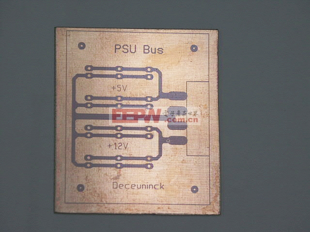
The developer in the tupperware should be used only ONCE! (use fresh developer for every new PCB to develop)
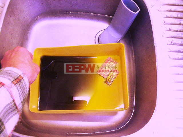
- A "tupperware" container to etch the PCB.
Etching of the PCB in a Ferric Chloride acid solution (Fe2CL3 + Water), available at electronics stores under the form of yellow-brownish grains to dilute in 1 liter of warm water, again in a "tupperware" container disposed in a "bain marie" (hot water recipient).
I use my kitchen sink filled with some hot water to obtain a temperature of about 50°C.
Ferric Chloride acid is more effective when its temperature rises, and therefore etching times decrease. Continuously moving the tupperware so that the etchant is flowing over the PCB also decreases drastically etching time. (with a fresh Ferric Chloride solution the etching time can go as low as 8-10 minutes).
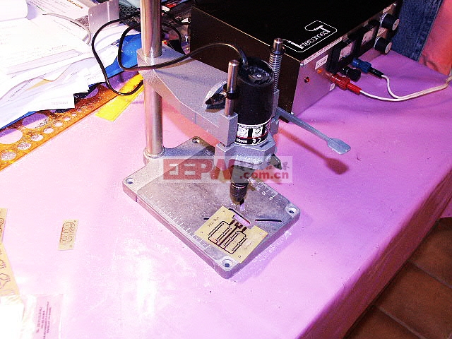
- A metalsaw and a minidrill.
After the etching process the PCB has to be cut, filed and sandpapered to the right dimensions.
Drilling of the PCB holes (OMG, I hate this...), beginning with a 0.8mm drill (suitable for resistors, little capacitors, transistors, IC’s, to 1.0, 1.2 1.3mm for bigger components.
I use a 12 to 18V - 100W Maxicraft mini drill and the accompanying drill standard (very easy) powered by my PWM speed controller for mini drills project.
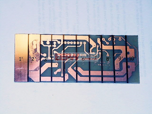
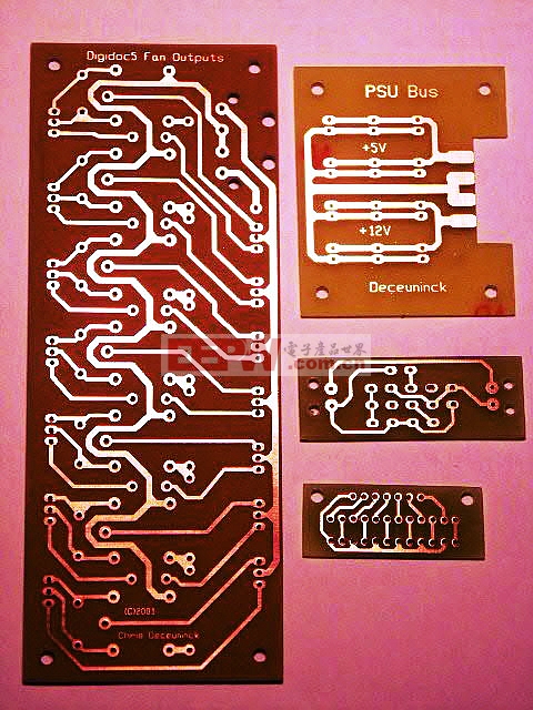
Some finished PCB’s:
Since the copper is still covered by the UV lacquer it’s protected against oxidation and moisture, and also the lacquer acts as a (not very good) solder flux when soldering the components to the PCB.
I prefer to remove the lacquer with aceton (ask your wife or girlfriend...), solder the components, and then treat the solder side with a spray varnish (I use transparent Plastic Spray 70 from Kontakt Chemie and green varnish from KF).
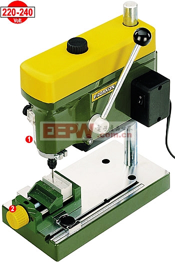
A few weeks ago I bought also a new TBM220 mini bench drill machine from Proxxonfor about 250 Euro.
Not cheap but very precise:
评论