NE5532驱动的30W功放-----30W POWER AMPLIFIER WITH NE5532


中国人写的,被外国人翻译成英语。
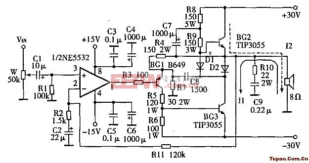
This is a band since held the role of the novel OCL amplifier circuit, the circuit schematic as shown in drawings by the NE5532 (You can also use other transport put) and two high-power NPN transistor. BG1/R4/R5/R6/R7 formed to promote the level, which R4/R7 determines the gain of the post-stage circuit. BG2/BG3/D1/D2/R8/R9/C7 constitute the output stage.
The circuit is characterized by static to impose a certain voltage output tube, it is the CPI bias state. This circuit distortion, high power, high efficiency.
Debug: static adjustment of R6, so that the the BG3 collector voltage of 0.6V can
评论