
How to Use the MAX15005 Curren

Abstract: This reference design shows how to use a MAX15005 automotive power-supply controller as a boost circuit to maintain a constant voltage during an automotive cold-crank condition.
The MAX15005 is a current-mode controller that operates from 4.5V to 40V. The device can manage cold-crank conditions and a load-dump condition as well. Once powered, the MAX15005 operates down to 2.5V, thus accommodating a further drop in the battery voltage.
This reference design shows a solution for a cold crank in automotive applications. The design includes the complete schematic, bill of materials (BOM), efficiency measurements, and test results.
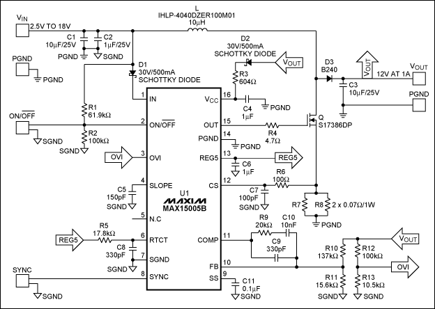
Figure 1. Schematic of the MAX15005B boost converter for FSW = 200kHz.
The BOM for this reference design is given in Table 1.
Table 1. Bill of Materials
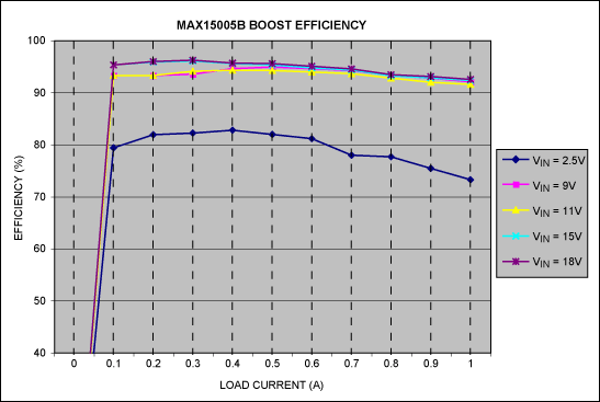
Figure 2. Load current vs. converter efficiency.
Converter output voltage and load current are shown in Figure 3 and Figure 4 with VIN = 2.5V and VIN = 11V, respectively.
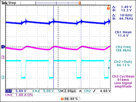
Figure 3. Converter output voltage and load current with VIN = 2.5V.
CH1: output voltage; CH2: MOSFET gate voltage; CH3: output current.
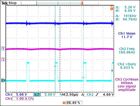
Figure 4. Converter output voltage and load current with VIN = 11V.
CH1: output voltage; CH2: MOSFET gate voltage; CH3: output current.
Introduction
When an automotive engine remains in a cold climate or is subjected to freezing temperatures for a long time, the engine oil becomes very viscous. In cold temperatures the battery’s internal resistance also increases from its normal value. If the engine is started during that time, the starter motor needs more torque, which draws more current from the battery. Due to transients in the current requirement and high-series resistance, the battery voltage can drop as low as 2.5V. This is known as the cold-crank condition in automotives.The MAX15005 is a current-mode controller that operates from 4.5V to 40V. The device can manage cold-crank conditions and a load-dump condition as well. Once powered, the MAX15005 operates down to 2.5V, thus accommodating a further drop in the battery voltage.
This reference design shows a solution for a cold crank in automotive applications. The design includes the complete schematic, bill of materials (BOM), efficiency measurements, and test results.
Specifications and Design Setup
The design uses the following specifications:- Input voltage: 2.5V to 18V
- Output voltage: 12V
- Output current: 1A
- Output ripple: ±0.6V
- Input ripple: ±15mV
- Efficiency: 75% with cold crank 90% for normal operation
- Switching frequency: 200kHz
Figure 1. Schematic of the MAX15005B boost converter for FSW = 200kHz.
The BOM for this reference design is given in Table 1.
Table 1. Bill of Materials
| Designator | Value | Description | Part | Footprint | Manufacturer | Quantity |
| C1 | 10µF/25V | Capacitor | GRM32DR71E106KA12L | 1210 | Murata® | 1 |
| C2 | 1µF/25V | Capacitor | GRM219R71E105KA88D | 805 | Murata | 1 |
| C3 | 10µF/25V | Capacitor | GRM32DR71E106KA12L | 1210 | Murata | 1 |
| C4, C6 | 1µF/16V | Capacitor | GRM188R71C105KA12D | 603 | Murata | 2 |
| C5 | 150pF | Capacitor | GRM1885C1H151JA01D | 603 | Murata | 1 |
| C7 | 100pF | Capacitor | GRM1885C1H101JA01D | 603 | Murata | 1 |
| C8, C9 | 330pF | Capacitor | GRM1885C1H331JA01D | 603 | Murata | 2 |
| C10 | 10nF | Capacitor | GRM188R71H103KA01D | 603 | Murata | 1 |
| C11 | 0.1µF | Capacitor | GRM188R71H104KA93D | 603 | Murata | 1 |
| D1 | 30V/500mA Schottky | Schottky diode | MBR0530T1 | SOD123 | On Semiconductor® | 1 |
| D2 | 30V/500mA Schottky | Schottky diode | MBR0530T1 | SOD123 | On Semiconductor | 1 |
| D3 | 40V/2A Schottky | Default diode | B240 | SMB | Diodes Incorporated | 1 |
| L | 10µH | Inductor | IHLP-4040DZER100M01 | IHLP-4040EZ | Vishay® | 1 |
| Q | 30V, 17A n-channel MOSFET | n-channel MOSFET | SI7386DP | Power PAKSO-8 | Vishay | 1 |
| R1 | 61.9K | Resistor | SMD 1% Resistor | 603 | Vishay | 1 |
| R2, R12 | 100K | Resistor | SMD 1% Resistor | 603 | Vishay | 2 |
| R3 | 604Ω | Resistor | SMD 1% Resistor | 603 | Vishay | 1 |
| R4 | 4.7 | Resistor | SMD 1% Resistor | 603 | Vishay | 1 |
| R5 | 17.8K | Resistor | SMD 1% Resistor | 603 | Vishay | 1 |
| R6 | 100 | Resistor | SMD 1% Resistor | 603 | Vishay | 1 |
| R7, R8 | 0.07Ω/1W | Resistor | LRCLR2010LF01R070J | 2010 | IRC | 2 |
| R9 | 20K | Resistor | SMD 1% Resistor | 603 | Vishay | 1 |
| R10 | 137K | Resistor | SMD 1% Resistor | 603 | Vishay | 1 |
| R11 | 15.6K | Resistor | SMD 1% Resistor | 603 | Vishay | 1 |
| R13 | 10.5K | Resistor | SMD 1% Resistor | 603 | Vishay | 1 |
| U1 | 4.5V to 40V input, automotive flyback/boost/SEPIC, power-supply controller | PWM controller | MAX15005BAUE+ | TSSOP-16 | Maxim | 1 |
Performance Data
The efficiency vs. load current plots for this design are given in Figure 2. Input voltage was the test parameter.Figure 2. Load current vs. converter efficiency.
Converter output voltage and load current are shown in Figure 3 and Figure 4 with VIN = 2.5V and VIN = 11V, respectively.
Figure 3. Converter output voltage and load current with VIN = 2.5V.
CH1: output voltage; CH2: MOSFET gate voltage; CH3: output current.
Figure 4. Converter output voltage and load current with VIN = 11V.
CH1: output voltage; CH2: MOSFET gate voltage; CH3: output current.
Murata is a registered trademark of Murata Manufacturing Co., Ltd.
On Semiconductor is a registered service mark of Semiconductor Components Industries, LLC.
Vishay is a registered trademark of Vishay Intertechnology, Inc.
评论